FPGA-Verilog-Beginners-Guide-Part-#1-thru-#5
July 17, 2018
[FiX-OptEdit-Needed]
Introduction
Learning electronics can be a bit challenging sometimes, but it is really fun if you have a little patience to read, understand and experiment. FPGAs need not be any different. Let us give it a try and see how fast and easily we can learn a little bit about FPGAs and create a simple working test project with this easy FPGA tutorial. To get the best out of this tutorial series, I strongly recommend to download the tools listed at the end of this document and try doing every step as you read along.
Some time back, I wanted to learn about programming FPGAs. I started googling only to find that there is no FPGA tutorial on the web (that is the case when this tutorial was originally written. But there should be more FPGA tutorials available online now!) that can get you started with learning a little bit of HDL and take you all the way through design, simulation, and implementation. There are many tutorials online that will help you learn HDLs, some tutorials tell you how to do simulation, some may tell you about implementation, but no single tutorial that guides you step by step from basics to implementation.
I decided to write this tutorial in the hope that it may help our readers to learn a little bit of Verilog (The HDL I chose to learn first because of its syntax similarity to C), simulate your code and implement it on real hardware. This tutorial expects you to have basic knowledge in Digital Electronics, Familiarity with some programming language (preferably C). This tutorial is not meant to be an in-depth study about Verilog or FPGAs or anything, but just a guide to walk you through different basic things you need to know to design a simple digital circuit in Verilog, simulate it and implement it on hardware.
We will be using
Xilinx ISE for simulation and synthesis. ISE Webpack version 14.7 is preferred, which is the latest version available (and last since Xilinx moved on to Vivado). If asked during installation, install “System Edition” because it will include Xilinx EDK as well. Please note that ISE Webpack and EDK licenses are separate. You will need ISE license installed to follow the next few parts of this tutorial. Please note that EDK evaluation license is only valid for 30 days but ISE Webpack license is perpetual. The final design will be programmed to an Elbert – Spartan 3A FPGA Development Board to make sure our code works on real hardware as well.
BTC
What is FPGA?
FPGA stands for “Field Programmable Gate Array”. As you may already know, FPGA essentially is a huge array of gates which can be programmed and reconfigured any time anywhere. “Huge array of gates” is an oversimplified description of FPGA. FPGA is indeed much more complex than a simple array of gates. Some FPGAs has built-in hard blocks such as Memory controllers, high-speed communication interfaces, PCIe Endpoints etc.. But the point is, there are a lot of gates inside the FPGA which can be arbitrarily connected together to make a circuit of your choice. More or less like connecting individual logic gate ICs (again oversimplified but a good mental picture nonetheless). FPGAs are manufactured by companies like Xilinx, Altera, Microsemi etc… FPGAs are fundamentally similar to CPLDs but CPLDs are very small in size and capability compared to FPGAs.
What are the applications of FPGA?
Architecturally FPGAs are essentially a sea of gates which can be reconfigured to build almost any digital circuit that one can imagine. This great flexibility along with the ability to reconfigure the device with different designs at-will makes FPGA a better choice compared to ASICs (Application Specific Integrated Circuit) for a lot of applications. For example, a deep learning, AI or application acceleration system can re-program a single FPGA with different algorithms at different times to achieve the best performance. An ASIC would not be as flexible in such situations. In certain applications, the number of individual units manufactured would be very small. Designing and manufacturing ASICs for these applications can be prohibitively expensive. In such situations, FPGA can offer very cost effective but robust solutions. Below are some of the potential applications of FPGAs in no particular order.
- Cryptography
- ASIC prototyping
- Industrial, medical and Scientific Instruments
- Audio/Video and Image processing and broadcasting
- High-performance computing, AI, and Deep Learning
- Military and Space applications
- Networking, packet processing, and other communications
What is FPGA programming?
FPGA programming or FPGA development process is the process of planning, designing and implementing a solution on FPGA. The amount and type of planning vary from application to application. But creating a requirements document that captures all specific requirements and creating a design document that explains how the proposed solution would be implemented can be very helpful to enumerate potential problems and plan around them. A little bit of time spent creating a quality design document will save tons of time in refactoring, debugging and bug fixing later. Implementing a solution on FPGA includes building the design using one of the design entry methods such as schematics or HDL code such as Verilog or VHDL, Synthesizing the design (Synthesis, netlist generation, place and route etc..) in to output files that FPGAs can understand and program the output file to the physical FPGA device using programming tools. Entering the design using schematics is not used in the industry widely anymore. So we will keep the discussion limited to design entry using HDL (Hardware Description Language), specifically Verilog in this article series. Synthesis and programming are almost completely taken care of the vendor tools such as ISE and Vivado and Numato Lab configuration tools. All necessary steps to be taken by the user as part of design entry, synthesis and programming will be explained in subsequent sections.
What is RTL?
RTL stands for Register Transfer Level. You might also encounter the terms Register Transfer Logic or Register Transfer Language, they all mean the same in the context of hardware designing. RTL is a higher level abstraction for your digital hardware design and comes somewhere between strictly behavioral modeling on one end and purely gate-level structural modeling on other ends. Behavioral modeling is explained in next articles in this series so don’t be daunted with this term. Gate modeling means describing hardware using basic gates which is quite tedious. RTL can also be thought as analogous to the term “pseudo-code” used in software programming. It is possible to describe the hardware design as sequences of steps (or flow) of data from one set of registers to next at each clock cycle. Therefore, RTL is also commonly referred to as “dataflow” design. Once the RTL design is ready, it is easier to convert it into actual HDL code using languages such as Verilog, VHDL, SystemVerilog or any other hardware description language. HDL and Verilog are explained in the next section. Check out the Wikipedia page on RTL for more information (
https://en.wikipedia.org/wiki/Register-transfer_level)
What is Verilog?
In the previous paragraphs, I mentioned the word “oversimplified” two times. The reason is that FPGAs are much much more than just a bunch of gates. While it is possible to build logic circuits of any complexity simply by arranging and connecting logic gates, it is just not practical and efficient. So we need a way to express the logic in some easy to use format that can be converted to an array of gates eventually. Two popular ways to accomplish this are schematic entry and HDLs (Hardware Description Language). Before HDLs were popular, engineers used to design everything with schematics. Schematics are wonderfully easy for small designs but are painfully unmanageable for a large design (think about Intel engineers drawing schematics for Pentium, which has millions of gates! it is unacceptably complex). If you have some electronics background, your initial tendency will be to use schematics to realize your design instead of learning a new language (This happened to me, honestly). For the aforementioned reasons, we will stick with HDL throughout this tutorial.
Verilog is a Hardware Description Language (HDL) which can be used to describe digital circuits in a textual manner. We will write our design for FPGA using Verilog (as if you write microcontroller programs in C and Assembly). Learning Verilog is not that hard if you have some programming background. VHDL is also another popular HDL used in the industry extensively. Verilog and VHDL share more or less same market popularity, but I chose Verilog since it is easy to learn and it’s syntactical similarity to C language. Once you are comfortable with Verilog, it should be easy learning VHDL as well. Want to read more about Verilog? Check out this wiki page (
http://en.wikipedia.org/wiki/Verilog) or check this tutorial (
http://www.asic-world.com/verilog/index.html).
What tools do we need?
1. A good text editor (I use
Notepad++ )
2. Xilinx ISE Webpack (
Download from Xilinx for free. Registration required).
3. A good FPGA development board (
Mimas V2 FPGA Development Board is used in the examples here. Picture of Mimas V2 is shown at the top of this page. If you have an
Elbert V2 Spartan 3A FPGA board, that should work perfectly too. There are some differences when setting up the project for Mimas V2 vs Elbert V2 but I will point them out when it is necessary.)
4. Mimas V2 or Elbert V2 Configuration downloader software (Required only if Mimas V2 /Elbert V2 FPGA Development Board is used. Download from the respective product pages)
Additional tools may be necessary to follow advanced topics in this series. Information about such tools will be shared ass they are needed.
Learning FPGA And Verilog A Beginner’s Guide Part 2 – Modules
63265 views April 29, 2016 admin 222
Learning Verilog itself is not a difficult task, but creating a good design can be. But we focus on simple designs here and I will try my best to explain things as simple as possible. If you had been programming with procedural languages such as C, C++, you will have to make up your mind to understand that not all things happen sequentially in the digital world. A lot of things happen parallel too. When I started learning Verilog, I used to write code sequentially as if I was writing a C program. C programs are running on microprocessors, which execute one instruction at a time sequentially. So it is easy to write a program in a way how you want things to happen one step at a time. And if you look closely, this is the weak point of microprocessors/microcontrollers. They can do only one thing at a time, one and only one thing (of course I’m talking about single core devices!). But unlike microprocessors, digital circuits (FPGAs, CPLDs, and ASICs) can do many things at the same time. And you need to learn how to visualize many things happening at the same time in contrast to many things happening at different times, one thing at a time, in a procedural language.
Verilog Modules
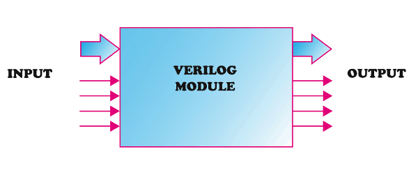
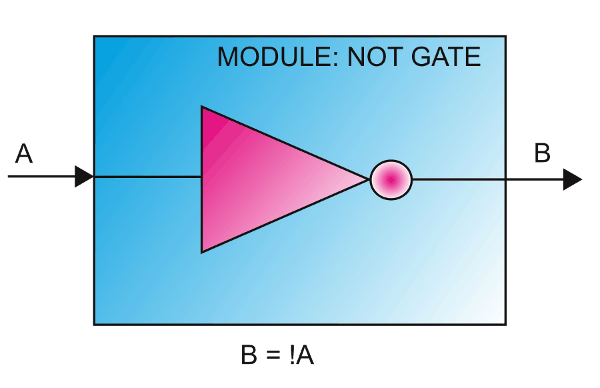
A Verilog module is a design unit similar to a black-box, with a specific purpose as engineered by the RTL designer. It has inputs, outputs and it functions as per its intended design. A simplest Verilog module could be a simple NOT gate, as shown in the second image below, whose sole job is to invert the incoming input signal. There is no upper bound on the complexity of the Verilog modules, they can even describe complete processor cores! Verilog deals with digital circuits. In Verilog realm, modules can be considered as equivalent to components in a digital circuit, as simple as a gate or a complex entity like ALU, counter etc… Modules are analogous to classes in C++ in a way that it is self-contained and give a finite number of methods (ports) to interact with the external world. Modules can be instantiated like classes are instantiated in C++ too. But beware; modules are not 100% similar to classes when it is implemented. For easy understanding, a module can be simply represented graphically as a box with a number of ports. The ports can be inputs, outputs or bidirectional. Ports can be single bit or multiple bits in width. The image below represents a module with a few inputs and outputs. The number of inputs and outputs, their width and direction will depend solely on the functionality of the module.
Fundamentally Verilog (or most HDLs for that matter) is all about creating modules, interconnecting them and managing the timing of interactions.
Enough talk, we didn’t even write a “Hello World” program yet. So how do we get our hands dirty with Verilog? Let us design a NOT gate in Verilog, simulate it and test it in a real hardware. A NOT gate (a.k.a an inverter) would be the simplest of all gates. The output of an inverter is always the negation of the input. ie; B = !A, where A is the input and B is the output. Below table summarize the behavior of NOT gate as a truth table.
INPUT
A
|
OutPUT
B = NOT A
|
|---|
0
|
1
|
1
|
0
|
NOT gate can be considered as a module with one input and one output with an internal behavior of B=!A. See the graphical representation of the inverter module below.
Let us see how we would represent this in Verilog.
module myModule(A, B);
    input wire A;
    output wire B;
    assign B = !A;
endmodule
Very simple, isn’t it? let us go through each and every line and try to understand what is going on in this bit of code.
The name of the module is “myModule” and is declared using the “module” keyword. The keyword module in Verilog defines our module (called myModule) and assign two ports to it. Everything that goes into this module is placed in between “module” and “end module” keywords. “myModule” has two ports. The ports’ size or direction is not known yet.
In the two lines below, port A and port B are declared as input and output respectively. I’m sure you are curious about what the keyword “wire” is doing there! Well, in Verilog there are two fundamental data types, ‘wire’ and ‘reg’. There are many other data types like int, real etc… But ‘wire’ and ‘reg’ plays very important roles in Verilog, that without learning them we cannot progress much.
As I mentioned before, knowing a little digital electronics will come handy here. ‘wire’ is just like a physical wire that we use to connect two different things electrically. If a potential is applied at one end of a copper wire, it will show up on the other end of the wire as long as you keep applying the potential. As soon as you remove the input, the potential is gone. This is true for a ‘wire’ data type in Verilog as well. A wire will have a particular logic state as long as it is driven by some other entity. If nobody is driving the wire, it will be in an unknown state. In Verilog, ‘wire’ can be used to connect things within a module or between two modules.
On the other hand, ‘reg’ can store a logic state and maintain it until someone changes it (think about a register in a microcontroller). This is similar to a flip-flop. If you put flip-flop in one state, it will remain in that state until somebody changes it.
So you can use wire as input or output for a module and ‘reg’ can be used as the output of a module. When wire is used as output, there should be a ‘reg’ that drives the wire from within the module so that ‘wire’ will have some meaningful information on it. If ‘reg’ is used as output, no other mechanism is necessary since it can hold data on its own.
Then why “myModule” has both input and output declared as wires? Good question, the answer is, because the module represents a NOT gate. Gates never store any state. Gates are purely combinational; i.e. its output always depends on the current input. If there is some logic state applied to its input then there will be a corresponding output (B = !A in this case). If no logic state is applied to the input it is considered as unknown state and the output state will also be unknown. And this also implies that to have any useful output from this module, some other entity should be driving its input from somewhere else (keep this in mind, we will touch this subject later when talking about test bench).
One more important thing about the above code is the keyword “assign”. The assign keyword is used to create combinational circuits. Whatever written in the right side of equal sign in the statement will be evaluated and the result will be assigned to the entity on the left side and this happens asynchronously. As soon as any changes happen on the right side, the result will be reflected on the left side. If you find it difficult to understand this, you may want to read a little about combinational digital circuits.
Now that we have a piece of code, we may want to simulate the code to see if it is working as expected. Simulation, in a broad sense, is the process of giving some known input and generating the corresponding output. The output is expected to be dependent on both the input and the behavior of the module under test. When the output is verified against expected output, it is called verification. There are many tools available for simulation and verification. Here we will be using iSim (part of Xilinx ISE Webpack) for simulation and waveform inspection.
Learning FPGA And Verilog A Beginner’s Guide Part 3 – Simulation
48394 views April 29, 2016 admin 127
Ok, we have a module and tools ready now, let’s try to run a simulation on the module and see if it works as expected. In order to simulate the module, we need to give some input to the module, how we do that? The answer is, we need to create a test bench! The test bench will generate the necessary inputs for the module under analysis (Here “myModule”). A test bench is nothing but another Verilog module which generates some signals and feeds it to the module under test. During simulation, the test bench should be a “top module” (top-level module) with no I/O ports. But when it comes to implementation on real FPGA, the “top module” can have I/O ports and test benches won’t be the top modules there (we will talk about this in detail later). So here goes the test bench code.
module myModule_tb();
    wire out;
    reg clock;

    always begin
 #1 clock =!clock;
    end

    initial begin
 //Initialize clock
 clock = 0;

 //End simulation
 #10
 $finish;
    end

    myModule notGate(clock, out);

endmodule
Let me break this down for you.
The test bench is just another module, with no I/O ports as I mentioned earlier. I have created a wire named “out” and a reg named “clock”. We will create a clock on reg “clock” by periodically inverting it and feed it to the input (port A) of myModule. The wire “out” is connected to the output port (port B) of myModule. The result should appear on the wire “out” in the simulation.
The “always” block is something worth special mention here. As the name implies, “always” block will keep on executing as long as the simulation is running. In real-world designs, “always” blocks are a little more complicated with sensitivity lists etc…. But for this simulation, the simplest form of “always” should suffice. I’ll discuss this in details in later chapters.
In the “always” block the reg “clock” is inverted after every one-time unit delay. The symbol # is a way to specify a delay in Verilog. So the always block executes always, and inside the block, “clock” is inverted continuously so that the waveform on clock looks like a square wave. Remember that # symbol is not a synthesizable element. We have to find some other way if delay needed in our design when we synthesize the code. But it works just fine for simulation.
The next block is an initial block. As its name suggests, this block will be executed only once at time t = 0. So anything that we need to initialize should go here. Initial block also is usually used only in test benches. Initial blocks are rarely used in synthesizable code, instead, reset logic is created if initialization is required. We initialize the reg “clock” to zero. This is very important. If we don’t initialize a register, its value is considered as unknown and no matter how many times an unknown is inverted, the result will always be unknown. That is, if we leave “clock” uninitialized, “clock” won’t be generated. The last part of the initial block is the $finish directive. The $finish directive is placed after a 10-time unit delay, this means after simulating the design for 10-time units, stimulator will stop running. All functions start with the $ symbol is called tasks. Tasks are merely commands to the simulator, they don’t alter the circuit behavior.
Last but not the least, the module instantiation. The statement “myModule notGate(clock, out)” creates an instance of the module “myModule” with name “notGate”. You can create as many instances as you want from a module. One really important thing here is the wiring. If you look at the code, you can see the reg “clock” placed as the first parameter and the wire “out” is placed as the second parameter. This literally means that the reg “clock” is connected to port A of the module instance and wire “out” is connected to port B of the module instance.
Now it is time to run the simulation. Follow the steps below to run the simulation in Xilinx ISE Webpack (Images are based on Xilinx ISE Webpack 14.7).
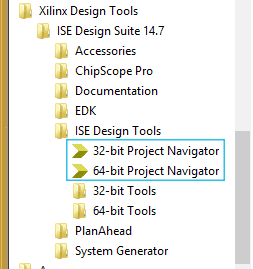
- Runs ISE Project navigator from the Windows program menu. Select 32 Bit or 64 Bit version of ISE depending on your Operating System.
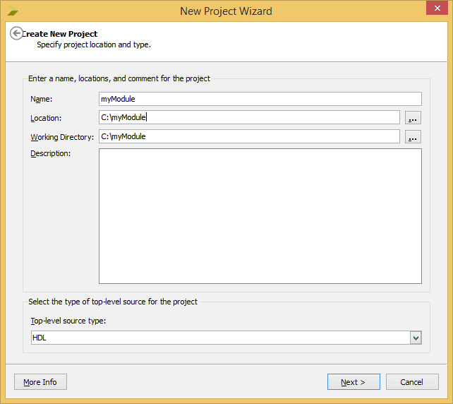
- From the File menu, select “New Project”
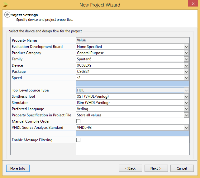
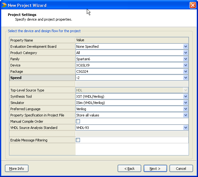
- Name your project and select a directory to save the project and click next (refer to the picture below).
- Change the project settings as required. You can select the FPGA family and device based on the board you use. For Mimas V2 Spartan 6 FPGA Development Board it should be set as in the image below. For Elbert V2 Spartan 3A FPGA Development Board, the device family will be “Spartan 3A and Spartan 3AN”, Device will be “XC3S50A”, Package will be TQ144 and Speed will be -4. Once the information is filled in, click next and then finish.
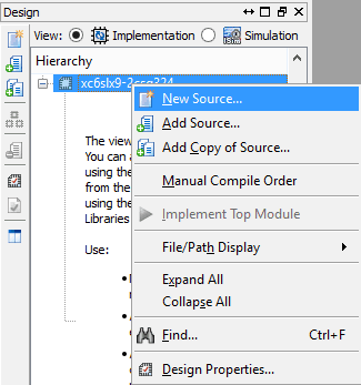
- We have created an empty project in Xilinx ISE Webpack. Now right click on the project and select “New source” from the pop-up menu.
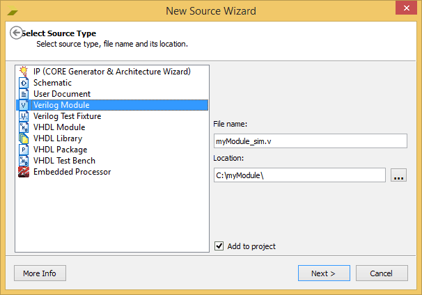
- Select “Verilog Module” as the source type and type in the file name as shown in the image below.
- Replace the autogenerated module template (or the contents of the whole file) with the code below.
module myModule_tb();
    wire out;
    reg clock;

    always begin
  #1 clock =!clock;
    end

    initial begin
  //Initialize clock
  clock = 0;

  //End simulation
  #10
  $finish;
    end

    myModule notGate(clock, out);
endmodule

module myModule(A, B);
    input wire A;
    output wire B;
    assign B = !A;
endmodule
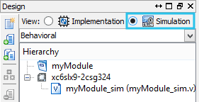
- Now make sure that we are in the simulation mode by selecting “Simulation” in design view
- Start simulation by right clicking on “Sim” process in the process view and selecting “Run” (The Verilog file myModule_sim.v must be selected in the Design View for this option to be visible).
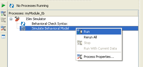
- Now the ISim simulator will start and you will be presented with a simulation waveform like the one below (Sometimes you may have to zoom in/out a little bit to see the waveform correctly).
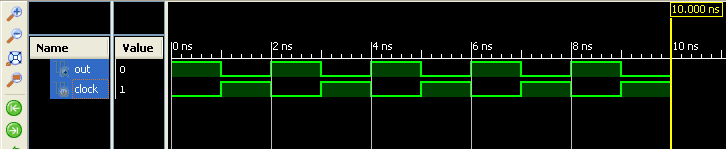
Inspect the waveform and make sure that our Verilog module is working as expected. As you can see in the image above, the output is the inverted form of the input clock. This is exactly what we expect from a NOT gate. In part 4 of this tutorial, we will implement this module on a real hardware.
Download complete Xilinx ISE simulation project for mimas V2
Download complete Xilinx ISE simulation project for Elbert V2
Learning FPGA And Verilog A Beginner’s Guide Part 4 – Synthesis
31740 views April 29, 2016 admin 71
So far we learned a few things about Verilog and how to create a module in Verilog and run a simulation. While simulation can tell us a lot of things about the correctness of our module, there is nothing like putting it on a piece of hardware and seeing it working. In this part of the tutorial, we will walk you through the steps for synthesizing the module and implementing it on
Mimas V2 Spartan 6 FPGA Development Board (or
Elbert V2 Spartan 3A FPGA Development Board) hardware.
As mentioned in part 3 of this tutorial, the test bench code is used only for simulation. To synthesize our module, we have to remove the test bench code. For those who don’t know, HDL Synthesis is the step where the HDL ( Verilog/VHDL or any other HDL for that matter) is interpreted and an equivalent hardware topology is generated. This hardware topology will be very specific to the target FPGA selected. Synthesis is a very complex process and we don’t need to know the internals to get our simple module up running.
We will use
Mimas V2 Spartan 6 FPGA Development Board to implement our module and the steps are very similar for
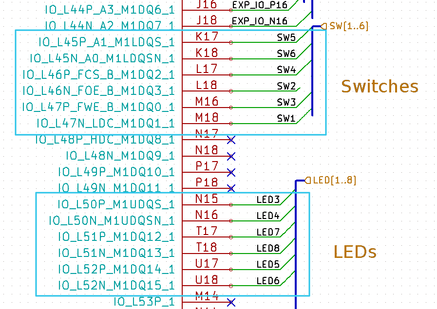
Elbert V2 Spartan 3A FPGA Development Board as well. Mimas V2 board has a Xilinx Spartan 6 FPGA, a DDR SDRAM and a few other peripherals on board. The exact FPGA part number used on this board is XC6SLX9-CSG324. This is a 324 pin CSG324 BGA chip with 9K logic cells. The image below shows the part of the schematics where FPGA IOs for LEDs and Push Button Switches are connected. We will use one Push Button Switch and one LED to implement our logic.
Let’s come back to our module and think about how we can implement the same on the hardware. The module in question is a NOT gate. As we know, the output of a NOT gate is always the negation of the input. We can have many possible hardware configurations to test this module. The easiest would be with a switch and a LED. See the proposed hardware configuration in the picture below.
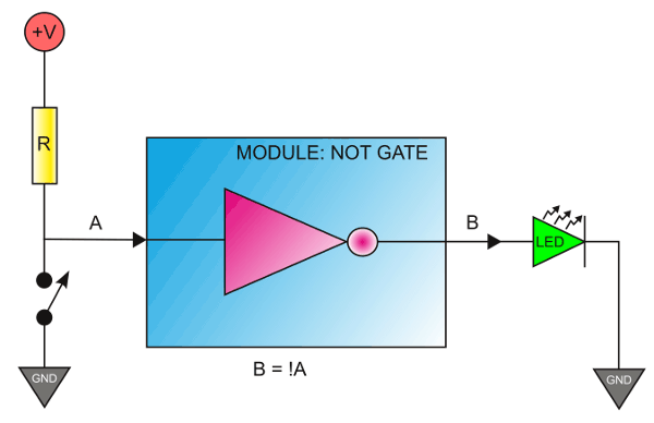
In the above diagram, a switch is connected to an input which is pulled up to VCC using a resistor. The output is connected to a LED. Let’s take a moment to understand how this circuit is going to behave. When the switch is in open position, there will be a positive voltage ie; a logic 1 at the input (A) of the NOT gate. That means the output (B) will be at logic 0. So the LED will be in OFF condition. When the switch is closed, the input of NOT gate will become logic 0 and the output will switch to logic 1 state. And the LED will glow.
Now we know the basic hardware requirements. We need the following in our prospective hardware.
- An input capable IO with a pull-up resistor and a switch attached.
- An output capable IO with an LED attached.
Let’s take a closer look at the Mimas V2 Spartan 6 FPGA Development Board. The following image shows the LED and switch we are planning to use on Mimas V2. Elbert V2 also has onboard switches and LEDs that can be used for this purpose. If you are using Elbert V2, LED8 and Switch SW5 would be good choices (The project attached at the tutorial for Elbert V2 uses SW5 and LED8).
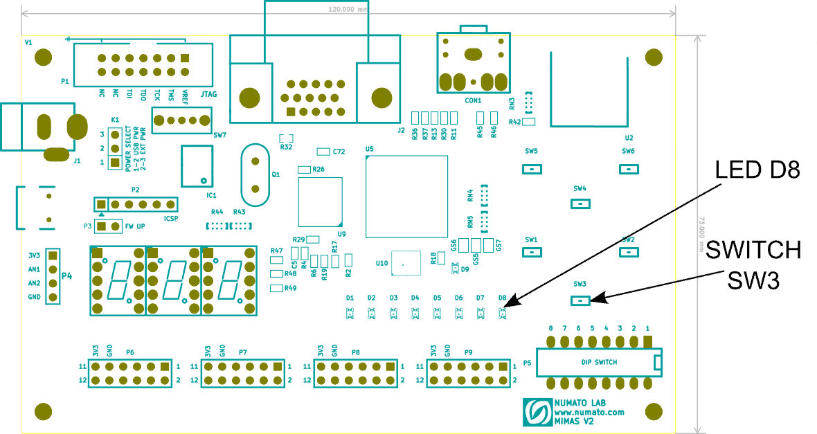
As we see in the image above, Mimas V2 has six general purpose push button switches and eight LEDs for the user’s convenience. We can now take a look at the Mimas V2 schematics and learn a little bit more about where the switches and LEDs are connected. Let’s choose push button switch SW3 and LED8 for our purpose. Looking through the schematics reveals that SW3 is connected to IO M16 and LED8 is connected to T18 of the FPGA respectively (M16 and T18 are not the IO names, rather they are the names of the BGA balls that the IOs are connected to.).
We now have a Verilog module that we want to implement and we have selected a hardware platform and decided what IOs to use for implementation. Let us revisit our module. I’m reposting the module code here.
module myModule(A, B);
   input wire A;
   output wire B;
   assign B = !A;
endmodule
Our module has two ports. Port A, which is the input and Port B, which is the output. An attentive reader would be asking now, how are we going to attach Port A to M16 of the hardware and Port B to T18 of the hardware. We will do this by defining user constraints. User constraints tell the router and the placement logic (which is a part of HDL synthesizer) on which physical pins the module signals are to be connected. We make a list of constraints and place it in a file and include that file in the project. This file is called a User Constraints File. For Xilinx tools, it is a text file with .ucf extension. Fortunately, the user constraints file for Mimas V2 is already available for download at the product page. This file has definitions for all IOs available on Mimas V2. But we don’t need all of them. So I’ll remove the unused part and post the required file contents here.
# User Constraint File for NOT gate implementation on Mimas V2
# Onboard LEDs
NET “LED” LOC = T18;
# Push Button Switches.
# Internal pull-ups need to be enabled since
# there is no pull-up resistor available on board
NET “SW” PULLUP;
NET “SW” LOC = M16;
The content of this file is pretty self-explanatory. On line No.4 it says the net LED (net is equivalent to wire/connection in the physical circuit) is connected to the physical pin T18. You might have noticed the NET “SW” PULLUP part. This means that the net SW will be pulled up to VCC. Many of the FPGA IOs have built in pull up resistors available. These resistors can be activated by appropriately mentioning it in the user constraints file. That is what exactly this particular line does. Line No. 11 connects the net SW to physical IO M16. Well, this still doesn’t answer how the ports of our module are going to be connected to the switch and LED. Like I have mentioned before, the ports of a module are equivalent to wires going in and out of the module. That, in turn, is equivalent to a net. So we can use the port names as net names in the user constraints file. So if we modify above user constraints code for our NOT gate module, it will look something like this.
# User Constraint File for NOT gate implementation on Mimas V2
# Onboard LEDs
NET “B” LOC = T18;
# Push Button Switches.
# Internal pull-ups need to be enabled since
# there is no pull-up resistor available on board
NET “A” PULLUP;
NET “A” LOC = M16;
You can download complete Xilinx ISE projects for Mimas V2 and Elbert V2 at the end of this page. The projects contain working ucf files.
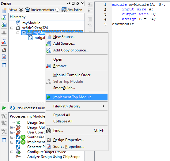
Now we have pretty much everything we need to synthesize the design and test it. Open our simulation project in Xilinx ISE Webpack and change the mode to Implementation and add the user constraints file in the project as shown in the picture below. Don’t forget to remove the test bench code from the Verilog source file and switch back to “implementation” mode in design view.
Save project and right click on the module and select “Implement Top Module” from the popup menu. Synthesis may take a few seconds to a minute. And if everything goes right you will see many green circles with a tick mark in the Process view right beneath the Hierarchy view (refer to the image below).
If any item turns yellow that means there is some kind of warning. Warnings are OK for time being. If any item turns red, there is something that went wrong. Please go back and verify all steps.
We have successfully synthesized the design. Now it is time to program the output on to the hardware. Our hardware platform Mimas V2 (and Elbert v2) requires bitstream (the final output of the synthesis process) to be in raw binary format. But ISE doesn’t generate raw binary bit file by default. We can do this by following the steps below.
- Right click on the “Generate Programming File” option in “Processes” window.
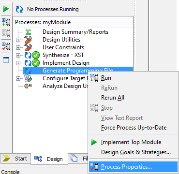
- Select “Process Properties” from the popup menu. In the dialog box, check “Create Binary Configuration File” check box and click “Apply”.
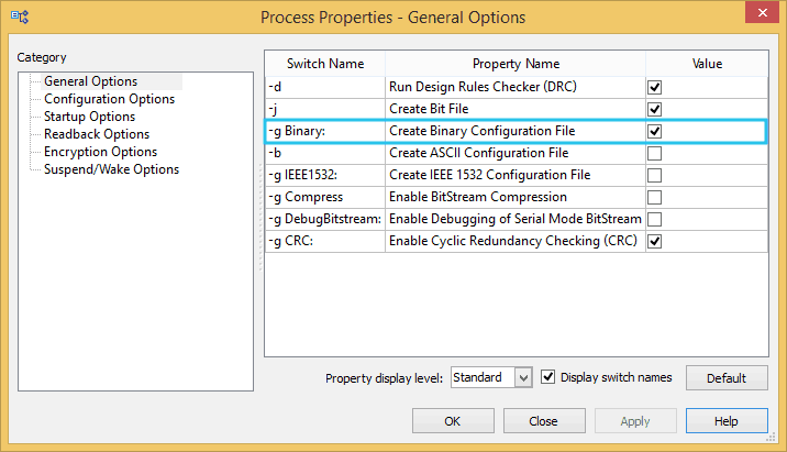
- Click “OK” to close the dialog box. Right click on “Generate Programming File” option in the process view on the left and select “Run”. Now you will be able to see a .bin file in the project directory and that file can be directly used for Mimas V2 configuration.
Now download myModule.bin (should be in the project directory if everything goes well) to Mimas V2 FPGA development board. Please see the Mimas v2 user manual to find more information about downloading output binary file to Mimas V2. Once downloading is complete, press the switch SW3 and you should see LED8 light up.
Download complete Xilinx ISE implementation project for mimas V2
Download complete Xilinx ISE implementation project for Elbert V2
Learning FPGA And Verilog A Beginner’s Guide Part 5 – Embedded System
24937 views April 29, 2016 admin 61
For many of us, learning FPGA was a natural next step from the world of micro-controllers and Embedded System. You learn the basics of Embedded System, do some projects using micro-controllers and microprocessors and one day realize that those devices may not be the best choice for a particular problem that you want to solve. A little research could lead you to FPGAs. But the FPGA world is very different from the micro-controller world you have seen so far. While micro-controller and Embedded System experience is very helpful, it can not help you get started with FPGAs without a somewhat steep learning curve. The tools are different, languages are different and even the programming paradigm is different.
But there is hope. By definition (in loose terms) FPGA is a bunch of logic elements that can be configured to make any logical circuit. If that is true, why not make a microprocessor out of those logic cells and program using traditional Embedded System friendly languages and tools? Yes, it is possible. But there is a question as to why this method of making a micro-processor or micro-controller out of FPGA logic is better compared to off the shelf micro-processors? There are many reasons why making microprocessor/controller in FPGA fabric is better (or worse) compared to an off-the-shelf micro. The most important reason is that you have access to the FPGA fabric from the micro-controller (through buses and peripherals created within the fabric, of course) and you can implement peripherals from a vast array of Xilinx’s freely available peripheral IPs or create your IP (or buy third-party IPs). It is possible to make pretty much any peripheral that you want within the capability of the FPGA that you have chosen to work with. There are a few important downsides to this scheme though. The total cost of hardware will be usually higher compared to an off-the-shelf micro for the same amount of raw processing power. If you can not find the peripheral IP that you are looking for, you will end up having to write one using Verilog or VHDL and you are back to square one (remember, what we wanted to do was not to deal with HDLs or FPGA workflow at all). It is possible to buy third-party IPs but depending on the specific IP, it can be very expensive. Also, it is worth mentioning that the tools required to build an embedded system out of an FPGA could set you back by a few hundred dollars.
Let us take a look at what a processor-based embedded system built into an FPGA would look like in it’s simplest form. As you can see in the diagram below, an embedded system built in FPGA fabric is not really different from any other embedded system. It has a processor, memory, buses, and peripherals etc. everything that you would expect in a normal Embedded System configuration. It is just that the processor, buses, and peripherals are all made by using logic cells that are available within the FPGA.
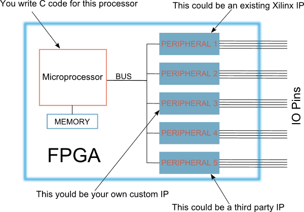
As you can see here, you could use a variety of peripherals from a variety of sources. The peripherals could be communication peripherals such as I2C, SPI, USART or signal processing cores such as FFT, filters or anything that you could imagine and implement on the FPGA fabric. This flexibility gives FPGA based embedded systems an edge in some situations compared to traditional microcontrollers where peripheral choices are often less flexible.
Embedded Infrastructure by Xilinx
Xilinx is arguably the world leader in FPGA and other programmable logic. They provide tools for building embedded systems around many of their FPGAs. Xilinx offers two kinds of fundamental options when it comes to implementing an Embedded System.
- Processor instantiated on FPGA fabric or so-called Soft Processors (Microblaze, Picoblaze)
- Hard processor on the die which has dedicated connectivity to FPGA fabric
As you can imagine, soft processors will use part of FPGA fabric to function and you have to be happy with what is left in order to implement your own peripherals. But with Hard processor cores, FPGA fabric is not used for implementing the processor and you will have 100% of FPGA fabric (or close to 100%) to implement your own peripherals. Hard processor cores are usually more powerful as well. But as of writing this article, the price of FPGAs with built-in hard processor cores tend to be higher.
During this tutorial we will stick with Soft processors, Microblaze to be specific. This is because Microblaze can be implemented on relatively inexpensive hardware such as
Mimas V2. Please note that Microblaze soft processor is not compatible Spartan 3 devices. So the information in this tutorial (Part 5) is not applicable to
Elbert V2 FPGA Development Board.
In simple terms developing an Embedded System with Xilinx FPGAs consists of the following steps.
- Create a Microblaze based embedded system project
- Add additional peripherals as necessary
- Configure the processor and other subsystems
- Build the processor core and all subsystems to generate a bit file that can be programmed to FPGA
- Create a software project that can run on the hardware ware infrastructure already made
- Write your own program in C and build
- Download everything to the FPGA and run
While it sounds a little complicated, Xilinx’s powerful tools make it very easy to implement those steps in practice. In fact, we will implement a working Embedded System with writing less than 10 lines of code. Now it looks like it is the right time to introduce Xilinx’s tools that we will use to accomplish the above steps. We will be using the following tools throughout the rest of this tutorial.
- Xilinx ISE Webpack 14.7 (http://www.xilinx.com/products/design-tools/ise-design-suite/ise-webpack.html)
- Xilinx Platform Studio
- Xilinx SDK
ISE is the primary FPGA design tool offered by Xilinx. This software includes an IDE and associated tools to implement HDL and realize it in hardware. Please see the previous parts of this tutorial to see some examples of how to create and build projects with ISE. Though it is important to have ISE installed on your system for Platform Studio and SDK to work, we will not be using the ISE IDE in this tutorial.
Xilinx Platform Studio and SDK together often called EDK (Embedded Development Kit). Xilinx Platform Studio is the tool you will use to design the hardware part of the embedded system (Processor, peripherals, buses etc..). Xilinx SDK is a software development environment based on Eclipse IDE. A lot of people will find the SDK tool visually very familiar because of this. Using SDK, you can create software projects and write C code that would run on the Embedded System designed using Platform Studio. Confused? don’t worry, everything will become much clearer when we go through the process step by step.
Xilinx ISE, platform Studio, and SDK can be downloaded and installed from
Xilinx website as a single package. But they are licensed separately. You will need one license for ISE Webpack (unlimited license but device limited, good enough for these tutorials) and another license for EDK (
Can be purchased here. Xilinx used to offer 30-day evaluation license. Please contact
Xilinx to find out more information). How to download, install and license these tools is beyond the scope of this tutorial. Please visit
xilinx.com to get more help on this.
Let’s get our hands dirty
To keep this tutorial concise and easy to follow, we will implement a simple Hello World Embedded System. Once implemented, it will print “Hello World” through the serial port. We will use
the Mimas V2 FPGA Development Board as the hardware platform to implement this project. Mimas V2 has a Spartan 6 LX9 FPGA and an onboard USB – Serial converter which would help us print data to the PC.
Step 1, Configuring and Building Microblaze Soft Processor and Peripherals
So far we have looked at some basics and selected a hardware platform. Now we will create a project using Xilinx Platform Studio and configure Microblaze based soft processor and some peripherals. Before we can create a project we must copy some supporting files to the EDK installation directory. These files will help us create and configure the project with a few simple mouse clicks. Download the
Base System Builder Wizard for Mimas V2 and extract the contents to the “board” directory within Xilinx EDK installation. If you have installed ISE/EDK 14.7 on C:\ drive, the whole path to these files will be C:\Xilinx\14.7\ISE_DS\EDK\board\NumatoLab\ipxact\MimasV2\data .
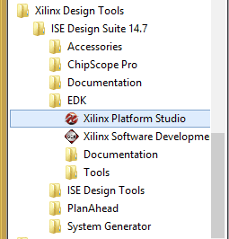
Now launch Xilinx Platform Studio from the start menu.
After Platform Studio GUI is loaded, click on File > New BSB Project. In the project Wizard window that shows up, enter a path and name for the new project. In the image below, “C:\embedded\HelloWorld\edk” is the path and “HelloWorld” is the project name.
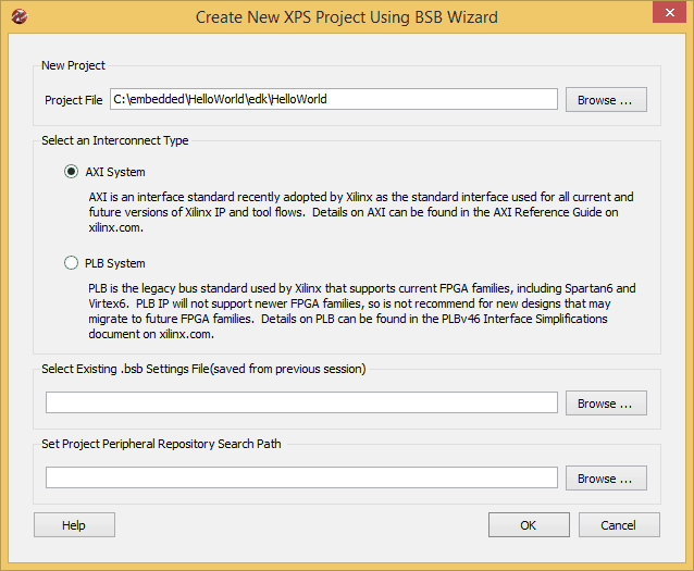
Click OK to continue. In the next window, select Nuamto Lab Mimas V2 as the development board. Leave all other settings to default. Refer to the image below for sample settings.
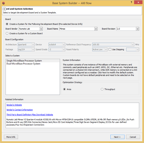
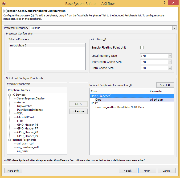
Click “Next” to continue. In the next Window, make sure that only UART is selected as peripheral as shown in the image below. Leave all other settings to default.
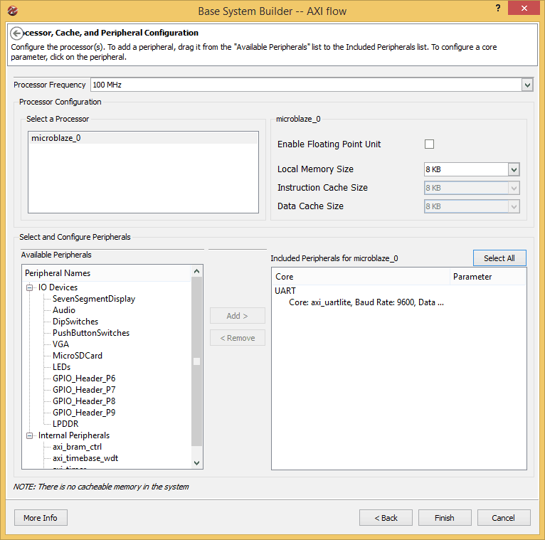
Click “Finish” to finish the wizard and generate the project. If everything went well, you will be presented with a window similar to the image below.
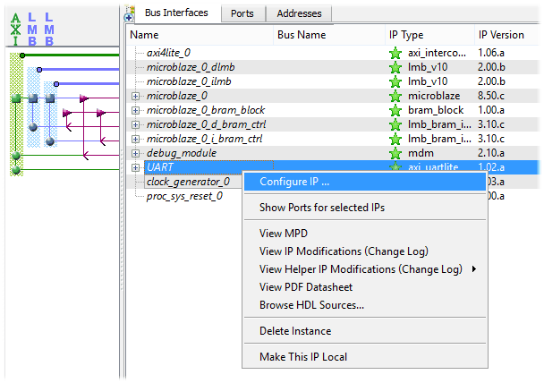
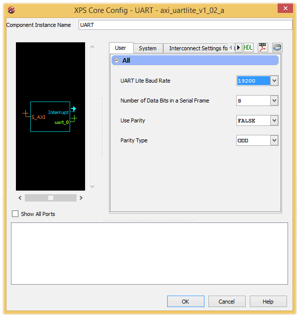
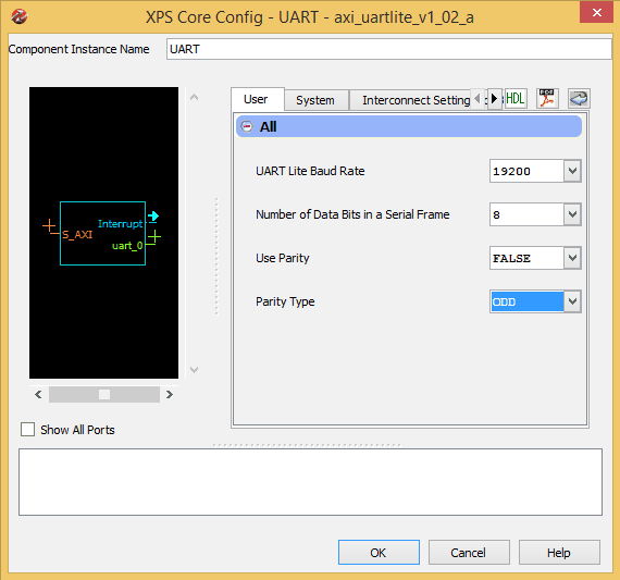
All IPs that are included in the project are configurable to suit your needs. But the only change that we need to make here to get this demo working is the UART Baud Rate. Right click on the UART IP and select “Configure IP” from the popup menu. In the IP configuration window, select 19200 baud rate and click OK. The images below show these steps.
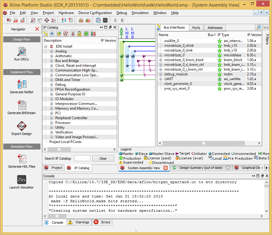
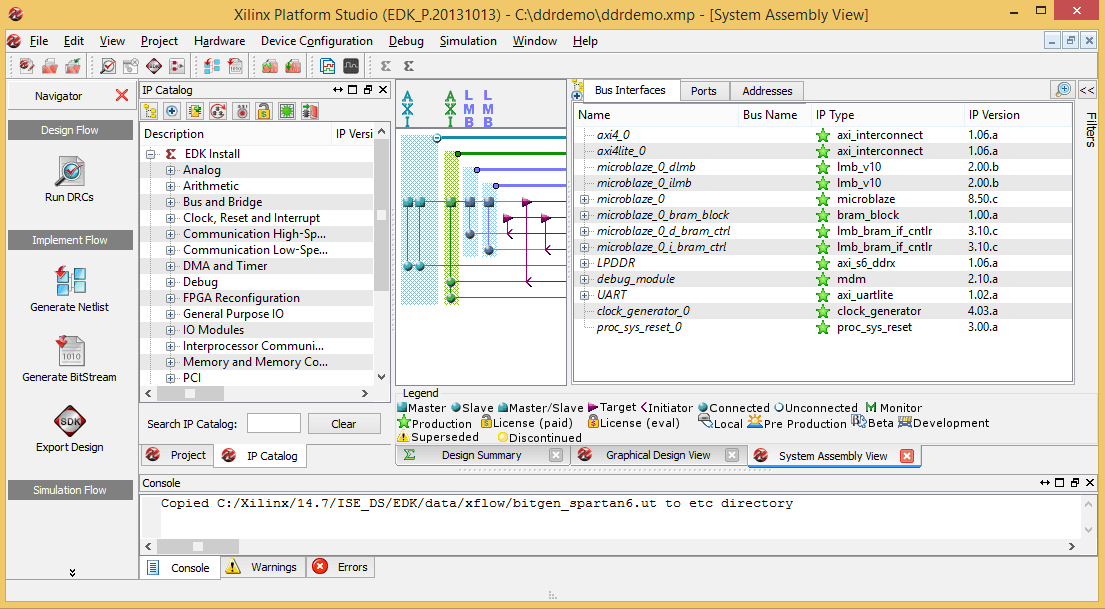
One more change that we need to make to the project is changing the startup clock. By default, XPS will set JTAG clock as FPGA startup clock. This is perfectly fine when we are using a JTAG adapter such as Xilinx Platform Cable – USB for programming FPGA. But to load FPGA configuration from SPI flash, we need to set startup clock to Cclk instead of JTAGCLK. To do this, go to the “Project” tab right next to the “IP Catalog” tab in XPS and open the Bitgen Options file “etc/bitgen.ut”. Change the line “-g StartUpClk:JTAGCLK” to “-g StartUpClk:CCLK”. Save the file and rebuild the project by clicking the “Generate bit file ” button on the left pane. It can take a few minutes for XPS to build the project. Once the build is completed successfully, you will see a message “Bitstream generation is complete. Done!”. If errors popup (ideally shouldn’t), fix them and rebuild. We are done with creating our embedded system hardware, it is that easy!
Now we can export the output files and create an SDK project. SDK is the tool that we will use to create a build application that will run on the Microblaze microprocessor. Click on the “Export Design” button in the left side toolbox in XPS. In the window that pops up, click “Export Only”. XPS will export all files necessary for creating an SDK project.
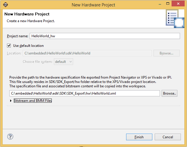
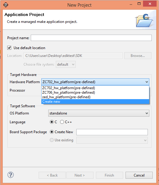
Now launch SDK by selecting “Xilinx Software Development Kit” from the start menu. Select a convenient folder as a workspace and click OK. To create a new project, click File > New Project > Application Project. The application Project Wizard will pop up and ask you to enter a project name a project name. We will call this project “HelloWorld”. In the same window, under “Target Hardware” section, click on “hardware Platform” Combo box and select “Create New”. The “New Hardware Project” wizard that pops up. Fill in a project name and click on the “Browse” button and navigate to our XPS project and find the folder SDK and select HelloWorld.xml (full path is SDK\SDK_Export\hw\HelloWorld.xml). Then click Finish. Please see the image below for an example.
Once a new hardware platform project is created, you will be sent back to the SDK Application project wizard. The newly created hardware platform will be selected in the application wizard automatically. The wizard should like as in the image below when everything is set-up properly.
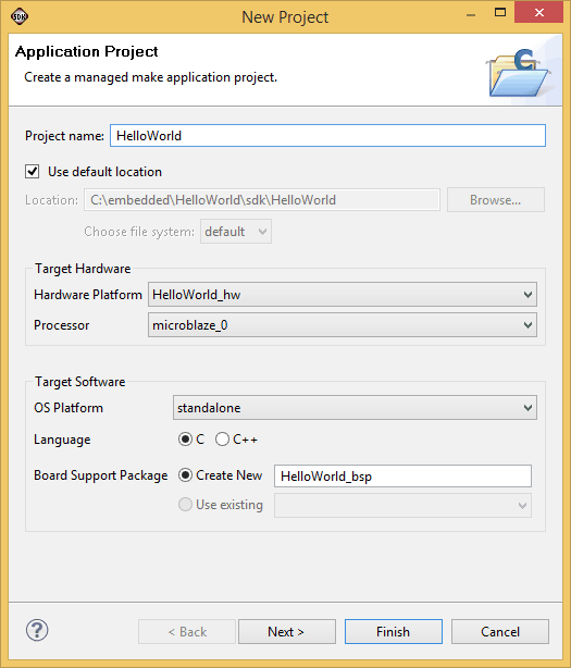
Click “next” and select “Hellow World” project template and then click “Finish”. Xilinx SDK will create the project and build it automatically. If everything went well, you should see “Build Finished” message in the build console.
There is a minor modification we need to do to the code at this point. The application generated using SDK will print “Hello World” a single time and exit. We want to change the application code so that the code will keep printing the data indefinitely. Find the print statement in the code (HelloWorld.c) and replace that with the following code.
while(1)
{
       print("Hello World\n\r");
}
All that we are doing here is to surround the print statement in a while loop so the printing never stops. Save the project and build.
Step 2, Generating bin file to download to Mimas V2
At this point, we have finished a major step. That is, creating and building a new project. The next step is to generate a single binary file that can be flashed to the SPI flash memory on Mimas V2 using Mimas V2 configuration tool. We will accomplish this with some command line tools that are installed with Xilinx ISE. To proceed, we need to find the following files that are generated by XPS/SDK.
- The bit file (The file name should be HelloWorld.bit if you used project name as in this tutorial. This file is located in the folder SDK\SDK_Export\hw inside the XPS project folder)
- The executable file (The file name should be HelloWorld.elf if you used project name as in this tutorial. This file is located in the folder SaturnV3test\Debug inside the SDK workspace folder)
- The .bmm file (The file name should be HelloWorld_bd.bmm if you used project name as in this tutorial. This file is located in the folder SDK\SDK_Export\hw inside the XPS project folder)
Once all these three files are copied to a common folder, open command line prompt and move to that folder. Follow the two steps below to generate the final bin file.
Step i
cmd> c:\Xilinx\xx.x\ISE_DS\settings64.bat
cmd> data2mem -bm HelloWorld_bd.bmm -bd HelloWorld.elf -bt HelloWorld.bit
Make sure to replace xx.x in the first command with your ISE version to form a correct path and use correct file names in the second command (if your XPS/SDK project names were different). If the commands did run successfully, you should see a new bit file generated in the folder (HelloWorld_rp.bit in my case).
Step ii
Now we need to generate a bin file. Run the following command in the same command window.
cmd> promgen -w -p bin -u 0x0 HelloWorld_rp.bit -spi -o download_me
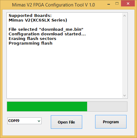
If the command was successful, you will see a few new files generated in the folder. One of the files will be download_me.bin. We will use this file to configure the Saturn Spartan 6 FPGA module. Run Mimas v2 flash configuration tool, select download_me.bin and click “program” button as in the image below (make sure to set the switch SW7 appropriately to allow flash download).
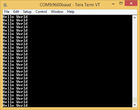
Put the switch SW7 on Mimas V2 to serial monitor mode and connect to the port using a serial terminal software (19200 baud). You should see the message “Hello World” being printed continuously.
Learning FPGA And Verilog A Beginner’s Guide Part 6 – DDR SDRAM
21102 views April 29, 2016 admin 73
Availability of sufficient data storage is a very important factor when selecting an FPGA development board. Various boards offer different memory options such as SRAM, QDR, SDRAM, FLASH etc. DDR SDRAM is most popular of all since it offers a reasonably large amount of volatile storage that can be accessed at a reasonable speed. An onboard volatile memory is key for a lot of applications such as image processing, data logging etc. since the Block RAM available in the FPGA logic fabric is very limited.
This article does not intend to visit the basics and architecture of SDRAM rather focus on how to create a very small project to show how to work with DDR SDRAM connected to an FPGA, specifically Xilinx Spartan 6. There are a lot of informative articles on the internet where a curious reader can learn about the inner workings of SDRAM. We found
this tutorial series very informative. Please note though that a deep understanding of the theory behind how SDRAM works is not necessary to follow this tutorial.
We will be using
Numato Lab’s Mimas V2 FPGA Development Board for this tutorial. But these steps can be applied to most other boards with minimal changes.
To make SDRAM work with an FPGA, we will need a few essential components.
- Memory Controller
- Wrapper logic
- User logic
Memory controller is the component that talks to the DRAM directly. This component generates the necessary signals (Address/Data/Control) to establish communication with the memory. Memory controller can be implemented in code or could be an IP block built into the silicon. Some FPGAs may not have a physical memory controller inside and the only way to interface DDR is to write code manually that uses FPGA logic resources. This takes up valuable space in FPGA logic that could otherwise be used for other purposes and also performance is usually not as good compared to hard IP memory controllers. A large number of FPGAs do have built-in hard IP memory controllers. Usually, these FPGAs are more expensive but built-in memory controller offers better throughput and less FPGA logic usage.
In most cases where memory controllers are available on silicon, the interface may not be readily usable by the user’s logic. In such cases, it is necessary to have a wrapper code that can interface with the memory controller core on one end and present a simple and consistent interface to the user logic. Usually, wrappers offer an interface consists of a number of ports that can be read/written by the user logic.
User logic is the final piece of the puzzle. The user code is the piece that generates, consume data. While working with the data, user logic may store the data temporarily on SDRAM (or any other memory device for that matter). For example, a data logging application running in FPGA may acquire samples from an ADC, store it in SDRAM. This data will be read back from the SDRAM and sent to a PC at a later time.
It may seem very complicated to get all this done. But don’t worry, there are tools that can help. Xilinx has done an excellent job of creating some nice tools that can help us generate all the above components and get our test application running with minimal or no manual coding. So you can forget about the stuff above for now, but this bit of knowledge is useful later when you are planning to use Memory Controller in a real-world project.
Let’s take a quick look at the board that we are going to use.
Mimas V2 has a Xilinx Spartan 6 LX9 FPGA in CSG324 package (has two built-in memory controllers) and a 512Mbit LPDDR SDRAM ( LP stands for Low Power and DDR stands for Double Data Rate). The FPGA’s CSG324 package is important here because Xilinx Spartan 6 LX9 is available in some other packages that don’t have a built-in memory controller. Of the two memory controllers available on the FPGA, one is connected to the 512Mbit LPDDR SDRAM and the other is left unused. All connections and other specific details are taken care of on the board, so no special hardware or accessories are needed to implement the projects we are going to do. For those who want to learn a bit deeper, we recommend looking at the Mimas V2 schematics (available at the end of the user manual) and
Xilinx Memory Interface Solutions User Guide. These documents are very valuable if one would want to learn beyond what is offered by this article.
Xilinx offers two different tools for implementing designs on Spartan 6 FPGAs depending on your workflow choice. They offer
ISE for conventional workflow and
EDK for Embedded System workflow. In the former case, all code will be implemented in RTL code such as Verilog/VHDL. In the latter case, a microprocessor and related peripherals including buses are built on top of FPGA logic (implemented using VHDL but most, if not all of it is automatically generated by Xilinx XPS) and the developer will write code in C that runs on the microprocessor. In this tutorial, we will visit both cases and see how to generate, build and test sample programs in both ISE and EDK environments.
Tool Version Compatibility and Help
This article uses Xilinx ISE and EDK version 14.7. So the screenshots and directions/commands may be different on your system if you are using a different version. Please adapt the steps mentioned in this article to make it work with your specific tool version. The best place to ask questions about ISE, EDK (XPS/SDK), Microblaze and Spartan 6 FPGA is Xilinx community forums at http://forums.xilinx.com/. You may optionally open a web case at http://www.xilinx.com/support/clearexpress/websupport.htm. Questions specific to Mimas V2 Spartan 6 FPGA Development Board may be asked at our forum or create a ticket if necessary at the
Contact Us page.
Creating, configuring and building memory controller core and test program on Xilinx ISE
You will need the following tools to implement this project.
- Xilinx ISE Webpack (Download here)
- Mimas V2 FPGA Development Board
- A USB Cable
- Mimas V2 Configuration Tool (Download from the product page)
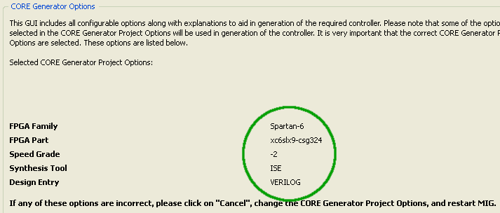
Start Xilinx ISE and select a new project from the File menu. The project wizard will pop up. Type in a project name and path in the first page. Select appropriate FPGA device in the second page. Mimas V2 has a Spartan 6 LX9 device (XC6SLX9). Settings, as shown in the image below, should work fine.
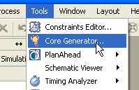
Click next and finish the wizard. Surprisingly we are not going to create or add any source files to the project and our use of ISE’s graphical user interface ends once we generate the required IP and other files using Coregen tool. To start Coregen tool, go to the Tools menu and select “Core Generator”.
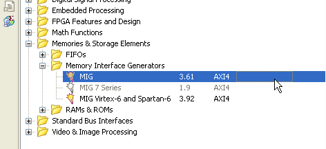
If Core Generator does not create a project automatically, create a project by selecting File>New Project. You will need to select the FPGA and its package when creating the project. Select Verilog as a design entry method. This is to make sure that Core Generator generates code in Verilog. In the IP catalog window, Find MIG under “Memory & Storage Elements” Category.
Double click to run Memory Interface Generator wizard. On the first screen, make sure that the selected FPGA device and other settings are correct. The settings should look like in the image below.
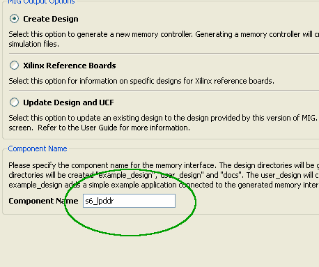
Click next to proceed to the next screen and type in a component name if necessary. Leaving the default name should work fine as well. For the sake of clarity, we will call our component “s6_lpddr”. Please replace this with the component name you chose when “s6_lpddr” appears later in this tutorial.
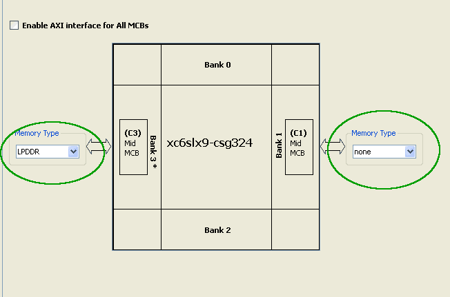
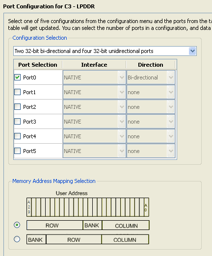
Click next to go to screen three of the wizard. Leave all options unchanged and proceed to screen 4. This screen is where we select the type of DDR memory and tell the MIG wizard where it is connected. Spartan 6 LX9 device has two memory controllers available. On Mimas V2 FPGA Development Board, the LPDDR device is connected to Bank 3 of the FPGA. Select LPDDR from the combo box corresponding to Bank 3. Leave Bank 1 settings unchanged. Settings on this page should look like as in the image below.
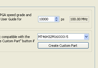
Click next to go to the next screen. This is the place where we select the DDR memory device and its operating frequency. Mimas V2 has onboard LPDDR memory which is Micron MT46H32M16 or equivalent. This device supports DDR clock up to 166MHz. Select MT46H32M16 memory device and set the clock period to 10,000. Clock period 10,000 corresponds to 100MHz DDR clock frequency. Though the DDR device supports up to 166MHz clock, we will use 100MHz to avoid the complication of messing with the PLL settings later. Mimas V2 has a 100MHz clock source and by using the same frequency for DDR clock, we can leave the PLL settings generated by MIG as is. Below is the image with correct memory part and frequency selected.
Click next to proceed to the next screen and leave all settings to its defaults. Click next again to proceed to the port configuration screen. Select Port 0 and leave rest of the ports unchecked as shown below.
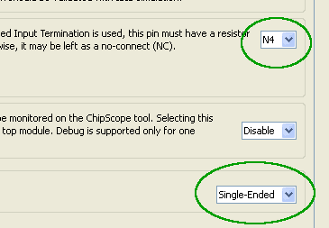
Click next to proceed to the arbitration configuration page. Since we are using only one port, there are no parameters to change on this screen. Click next again to proceed to FPGA Options screen. Select N4 as RZQ pin location and select Single Ended as system clock input. See image below with correct settings.
Click the next button a few more times and finish. Core Generator will generate a bunch of files. These files can be found under the directory \ipcore_dir\s6_lpddr (Assuming you used the name “s6_lpddr” for the auto-generated component). You will see three folders here, docs, example_design and user_design. docs folder has some very important documentation that can be used to learn more about Spartan 6 Memory Controller and the IP generated by MIG. Keep them for a later read.
Editing user constraints
Right now we are going to use the example design generated by MIG. The example design can be found (unsurprisingly) under the folder example_design. There are a few folders and files inside the example_design folder. rtl folder has all the Verilog files generated by MIG. par folder contains some batch files and scripts to build the example design. The user constraints seem to be auto-generated to match with Xilinx’s own development boards. Some changes are necessary to make the auto-generated code work with Mimas V2. Before building the project, we need to do the following.
- Edit the ucf file to make it usable with Mimas V2
- Configure the build environment to generate a binary configuration file
Go to par folder and find example_top.ucf. Open example_top.ucf using any text editor of your choice. Make the following changes.
- Change the line CONFIG VCCAUX=2.5; to CONFIG VCCAUX=3.3; . This change is necessary because Mimas V2 uses 3.3V for VCCAUX.
- Change the following lines
NET “error” IOSTANDARD = LVCMOS18;
NET “calib_done” IOSTANDARD = LVCMOS18;
NET “calib_done” LOC = “B2” ;
NET “error” LOC = “A2” ;ToNET “error” IOSTANDARD = LVCMOS33;
NET “calib_done” IOSTANDARD = LVCMOS33;
NET “calib_done” LOC = “T18” ; #LED1
NET “error” LOC = “T17” ; #LED2
Above changes will make the “error” and “calib_done” pins operate at LVCMOS33 IO standard and assign the nets to T18 and T17 of FPGA where LED1 and LED2 are connected. This will cause LED1 to turn on when calibration is done and LED2 to turn on if memory test failed
- Change the linesNET “c3_sys_clk” IOSTANDARD = LVCMOS25;
NET “c3_sys_rst_n” IOSTANDARD = LVCMOS18;ToNET “c3_sys_clk” IOSTANDARD = LVCMOS33;
NET “c3_sys_rst_n” IOSTANDARD = LVCMOS33;
Above change will set the IO standards for clock input and reset input to LVCMOS33. This is again because the bank that these IO belongs is powered by 3.3V rail.
- Add a line NET “c3_sys_rst_n” PULLDOWN;
This will enable pull down on the reset pin and will keep the memory controller our of reset without having to use any external components. Despite the name “c3_sys_rst_n”, MIG seems to be configuring reset input as active high.
- Change “c3_sys_clk” and “c3_sys_rst_n” pin assignments as below.
NET “c3_sys_clk” LOC = “V10” ;
NET “c3_sys_rst_n” LOC = “M16” ;
This will assign correct IO pads for clock input and assign switch SW3 as reset input.
We are done with the changes in ucf file now. This may seem difficult but easy enough if done carefully. It is a good idea to back up your original ucf file before saving the changes just in case if you want to go back and restart again.
Building the code
Next step is to modify the build environment to generate a binary configuration file. This is a very easy step to do. Find the file mem_interface_top.ut and open it in a text editor. Find the line “-g Binary:no” and change it to “-g Binary:yes” and save.
Now we are ready to build the project. Before building the project, make sure that the path to Xilinx build tools is added to PATH environment variable. Usually, the path is C:\Xilinx\\ISE_DS\ISE\bin\nt assuming ISE is installed on C: drive.
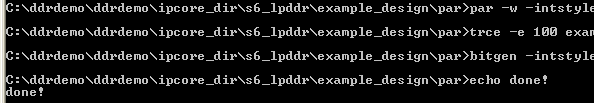
Now run the batch file ise_flow.bat by double-clicking the file or by using the command prompt. If everything went fine so far, the batch file will run the necessary tools to build the project and you will end up with a “Done” message and a bunch of new files in the par folder. The message should look like in the image below.
If the build process fails, refer to ise_flow_results.txt for more details on the causes of failure. You should see the file “example_top.bin” in par folder if build succeeded. This is the file we are going to program Mimas V2 Spartan 6 FPGA development board with.
Configuring Mimas V2 and testing
Programming Mimas V2 Spartan 6 FPGA development board is very easy. Download the latest version of the Configuration Downloader Application from the product page. Run the executable, no installation required. Load the binary file and program the flash as illustrated in the image below.
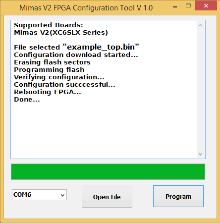
Watch the log window and confirm the configuration binary file is downloaded successfully. Now we are ready to test if the memory interface is working.
Testing if the example program we built, is very easy to do. You may remember we changed a few lines in the ucf file. Below are two of those lines.
NET “calib_done” LOC = “T18” ; #LED1
NET “error” LOC = “T17” ; #LED2
The first line assigns the FPGA pin T18 to the net “calib_done” net and the second line assigns FPGA pin T17 to “error” net. These FPGA pins are connected to LED1 and LED2 respectively. To verify proper functioning of the example program, all that we need to do is to check and make sure that LED connected to “calib_done” (LED1) turns on after power-up, indicating successful completion of initial calibration and the LED connected to “error” (LED2) stays off.
If you have observed calib_done going high and error stays low for a while, congratulations, you’ve got your Spartan 6 DDR SDRAM test project working. Thanks to Xilinx Memory Interface Generator for generating complete and ready to go code.
Creating, configuring and building memory controller core and test program on Xilinx EDK
It is quite easy to generate and build a simple sample program that can test the DDR SDRAM using ISE and it certainly is exciting. It would be more exciting if we could test the whole memory and print the output through UART. Yes, it is possible to do that using Xilinx EDK. And also you could write simple C code to access the DDR SDRAM. We will show you how!
You will need the following tools to implement this project.
- Xilinx EDK (More info here)
- Mimas V2 FPGA Development Board
- A USB Cable
- Mimas V2 Configuration Tool (Download from the product page)
What is Microblaze?
Microblaze is a 32-bit soft processor IP that is developed by Xilinx for their mid – high-end FPGA devices. Microblaze is compatible with their Spartan 6, Virtex and Zynq devices. You can find more resources including datasheet for Microblaze at Xilinx’s Microblaze page. Fortunately, we do not need to download Microblaze IP separate since it is bundled with Xilinx EDK tool. Microblaze based embedded design can use either PLB or AXI as the bus system. Since Xilinx is planning to phase out PLB and keep only AXI in the future, we will stick With AXI for our designs. You do not need deep knowledge of Microblaze or AXI to follow this article and build a working system successfully.
What is AXI?
AXI stands for Advanced eXtensible Interface. AXI is a bus interconnect based on ARM’s popular AMBA bus architecture. In a Microblaze based embedded system, AXI connects the microprocessor to all available peripherals. The only exception is Block RAM which is attached to the processor through LMB (Local Memory Bus). AXILite is available for connecting low throughput peripherals to the system such as UART, GPIO etc… AXILite uses fewer logic resources on FPGA compared to AXI. Usually, AXI is used to connect high throughput peripherals such as DDR memory, Ethernet etc.. Again, a detailed understanding of AXI is not required for following this article. But for the curious readers,
AXI Reference Guide is available here.
What is EDK?
EDK is a set of development tools provided by Xilinx to help create Microblaze based embedded system and develop software for the system. Xilinx EDK has two main components.
Xilinx Platform Studio (XPS)
Xilinx Software Development Kit (SDK)
These are the two separate software tools that we will use to design and implement our system. XPS is the tool used for designing and generating the hardware system. You will create and configure Microblaze processor and necessary peripherals using XPS and generate a bit file from the design. This bit file will be programmed to the FPGA to complete the hardware design. SDK is the tool where the software is written for the Microblaze processor. The software can be written using C or C++. SDK and XPS together will generate all necessary header files and linker scripts needed to successfully build the software for your system. We will take a detailed look at these tools as we go forward.
More details about these tools can be found here.
Creating Microblaze Based Embedded Hardware Platform
In this section, we will see how to create a basic Embedded Platform based on Microblaze using Xilinx Platform Studio (XPS). We will use the base System Builder (BSB) wizard to generate the system. To use BSB to generate a system for Mimas V2, you will need to download the BSB System Wizard files from the
product page and extract to the folder “C:\Xilinx\xx.xx\ISE_DS\EDK\board”. Once extracted, the complete path to the file should look like “C:\Xilinx\xx.xx\ISE_DS\EDK\board\NumatoLab\ipxact\MimasV2\data”. Once files extracted properly, go to All Programs > Xilinx Design Tools > EDK and click on Xilinx Platform Studio icon. Once XPS is loaded, click on “New BSB Project” under File menu or press Ctrl + Shift + B to invoke the BSB wizard. If everything went fine, the BSB wizard window will pop up as shown below.
Enter the path to a folder where you want to store the project and type in a project name. Select AXI System in the “Interconnect Type” section and click OK. In the next page of the wizard, select “Numato Lab” from the board Vendor combo box (This option should be available if you have placed the BSB wizard support files for Mimas V2 correctly as mentioned earlier). Select Mimas and 2.0 from Board Name and Board version combo boxes respectively and click the “Next” button.
You can set the Optimization strategy to Area or Throughput. We will leave it at the default option “Area” for this example. Click Next to proceed to the next page of the wizard. In the next page, you will have an option to select peripherals as shown in the image below.
Leave everything in this page to its defaults and click Finish. At this point, XPS will generate the system for you and you will be presented with a window like below.
This window shows all IPs available, IPs used in the design and bus connections between the IPs used. Here you may notice that DDR memory is connected to the Microblaze processor through AXI bus since DDR requires better throughput. But all other peripherals are connected to AXI Lite. To make this system work with Mimas V2 there is certain customization we need to do.
Change baud rate
The first change we need to make is the UART baud rate. Right click on the UART IP in the “Bus Interfaces” view and select “Configure IP”. In the IP configuration window that pops up, select baud rate “19200” and leave all other settings to defaults. Please see the image below to exact settings.
Connect RESET to an external switch
Next thing we need to do is to assign a switch to the “RESET” net of the Microblaze processor so we can reset the whole system when necessary. To do this, open the file “ddrdemo.ucf” file in the project view and replace the line
NET “RESET” PULLUP;
with
NET “RESET” LOC = M16 | IOSTANDARD = LVCMOS33 | DRIVE = 8 | SLEW = FAST | PULLUP;
This will connect the momentary switch SW3 on Mimas V2 to the Processor’s RESET line. This will allow us to reset the processor anytime by pressing switch SW3.
Select CCLK as configuration clock
By default, XPS will set JTAG clock as FPGA startup clock. This is perfectly fine if we are using a JTAG adapter such as Xilinx Platform Cable – USB for programming the FPGA. But to use Mimas V2 Configuration utility, we need to set startup clock to CCLK instead of JTAGCLK. To do this, go to the “Project” tab right next to the “IP Catalog” tab in XPS and open the Bitgen Options file “etc/bitgen.ut”. Change the line “-g StartUpClk:JTAGCLK” to “-g StartUpClk:CCLK”. Save the file click on the “Generate Bitstream” button on the left to compile the system and build the bitstream. This step may take a few minutes to a few tens of minutes depending on the speed of your computer.
Once the bit file is generated successfully, click on the “Export Design” button on the toolbar on the left. Click on the “Export Only” button on the window that pops up. This step will export all necessary files for creating an SDK project into a convenient directory (usually inside SDK\SDK_Export\hw under the current project directory). At this point, we have the hardware system ready. This is more or less equivalent to having a microprocessor/microcontroller board without and code written for it. So our next step is to write some code and build it.
Creating an Application program for Microblaze
We will use Xilinx SDK to write and compile code for the hardware platform we just built. Xilinx SDK is an Eclipse-based IDE that can create, build, debug and maintain projects for Xilinx Microblaze based platforms. To start SDK, go to All Programs > Xilinx Design Tools > EDK and select “Xilinx Software Development Kit”. When asked to choose a workspace, enter a convenient directory where you would like the projects files to be stored. To create a new SDK project, select “New Application Project” from File menu. You will be presented with a window like shown below.
Select create new from the Hardware Platform combo box. A new window will appear where we need to create a new Hardware Project.
Click on the Browse button and browse to the directory where the XPS project was saved earlier. And browse to SDK\SDK_Export\hw and select ddrdemo.xml. This wizard will automatically populate a project name, we will leave it unchanged. Click Finish button to go back to the Application Project Wizard. Back in the application project wizard, enter a project name and leave all other settings to defaults as shown in the image below.
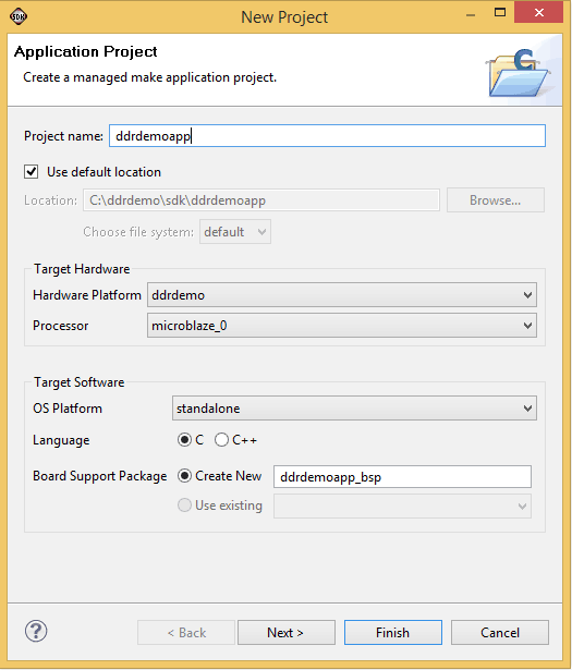
Click next to go to the last page in the application project Wizard. Select “Memory Test” template from the list of templates and click Finish. SDK will create a workspace and add three projects to it. All projects can be viewed in Eclipse Project Explorer as below.
In the image below, you can see three projects. Project on the top is the hardware platform. These files are copied directly from the directory where XPS exported the hardware system to. The one below is the application project that we will be working on. And the one all the way to the bottom is the BSP project which was automatically generated by SDK. The libraries and include files necessary for our application to work are stored under this project.
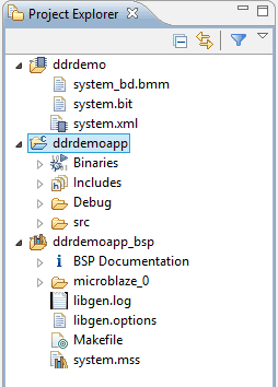
To build the project, select “Build All” from Project menu. If everything went fine so far, the project should build with no errors. Again this is a working project which can be downloaded and tested on hardware without any modifications. If you would like to see the code, go to src folder under the ddrdemoapp project and open the source files listed there. memorytest.c has the main() function.
Building And Testing The Program
Once the project is successfully created, SDK will build the program on its own. You can force another build by selecting “Build All” from the “Project” menu or pressing Ctrl+B.
Now that we have created and built the projects on XPS and SDK, we can create the final binary image. The idea is to use Xilinx data2mem tool to merge the FPGA bit file generated by XPS for Microblaze system and the executable generated by SDK.
We need to find the following files from the XPS and SDK projects that we have built.
- The bit file (The file name should be ddrdemo.bit if you used the same project name as mine. This file is located in the folder SDK\SDK_Export\hw inside the XPS project folder)
- The executable file (The file name should be ddrdemoapp.elf if you used the same project name as mine. This file is located in the folder ddrdemoapp\Debug inside the SDK workspace folder)
- The .bmm file (The file name should be ddrdemo_bd.bmm if you used the same project name as mine. This file is located in the folder SDK\SDK_Export\hw inside the XPS project folder)
Once all these three files are copied to a common folder, open command line prompt and move to that folder. Follow the two steps below to generate the final bin file.
Step 1
cmd> c:\Xilinx\xx.x\ISE_DS\settings64.bat
cmd> data2mem -bm ddrdemo_bd.bmm -bd ddrdemoapp.elf -bt ddrdemo.bit
Make sure to replace xx.x in the first command with your ISE version to form a correct path and use correct file names in the second command (if your XPS/SDK project names were different). If the commands did run successfully, you should see a new bit file generated in the folder (ddrdemo_rp.bit in my case).
Step 2
Now we need to generate a bin file. Run the following command in the same command window.
cmd> promgen -w -p bin -u 0x0 ddrdemo_rp.bit -spi -o download_me
If the command was successful, you will see a few new files generated in the folder. One of the files will be download_me.bin. We will use this file to configure Mimas V2. Run Mimas V2 flash configuration tool (make sure to set the slider switch on Mimas V2 into programming mode, please see details in the user manual), select download_me.bin and click “program” button as in the image below.

Once the board is programmed, put the slider switch on Mimas V2 into normal mode and connect to the COM port corresponding to the board using any serial terminal emulation software such as Hyperterminal or TeraTerm. Then press the switch SW3 to reset the processor. If everything went well so far, you should see the following test results printed on the terminal.
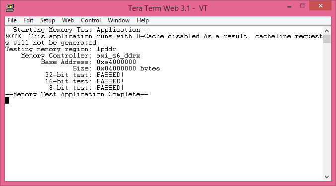
This tutorials shows how easy it is to generate and build simple test applications to exercise the DDR SDRAM available on Mimas V2 FPGA Development Board (or any other Spartan 6 based board for that matter).
10 Ways To Program Your FPGA
Adam Taylor
6/10/2016 09:47 AM EDT
21 comments

6 saves
Login to Rate
 Tweet
Tweet
Despite the recent push toward high level synthesis (HLS), hardware description languages (HDLs) remain king in field programmable gate array (FPGA) development. Specifically, two FPGA design languages have been used by most developers: VHDL and Verilog. Both of these “standard” HDLs emerged in the 1980s, initially intended only to describe and simulate the behavior of the circuit, not implement it.
However, if you can describe and simulate, it’s not long before you want to turn those descriptions into physical gates.
For the last 20 plus years most designs have been developed using one or the other of these languages, with some quite nasty and costly language wars fought. Other options rather than these two languages exist for programming your FPGA. Let’s take a look at what other tools we can use.
C / C++ / System C
 Click here for larger image
The C, C++ or System C option allows us to leverage the capabilities of the largest devices while still achieving a semblance of a realistic development schedule... although that may just be my engineering management side coming out.
The ability to use C-based languages for FPGA design is brought about by HLS (high level synthesis), which has been on the verge of a breakthrough now for many years with tools like Handle-C and so on. Recently it has become a reality with both major vendors, Altera and Xilinx offering HLS within their toolsets Spectra-Q and Vivado HLx respectively.
A number of other C-based implementations are available, such as OpenCL which is designed for software engineers who want to achieve performance boosts by using a FPGA without a deep understanding of FPGA design. Whereas HLS is still very much in the area of FPGA engineers who want to increase productivity.
As with HDL, HLS has limitations when using C-based approaches, just like with traditional HDL you have to work with a subset of the language. For instance, it is difficult to synthesize and implement system calls, and we have to make sure everything is bounded and of a fixed size.
What is nice about HLS, however, is the ability to develop your algorithms in floating point and let the HLS tool address the floating- to fixed-point conversion.
As with many things, we are still at the start of the journey: I am sure over the coming years, we will see HLS increasingly used in different languages, making HLS similar to very low level of a software engineer’s C.
More info:
PDF: Spectra-Q
PDF: Vivado HLx
10 FPGA dev tools:
Page 1: C / C++ / System C
Page 2:
MyHDL
Page 3:
CHISEL
Page 4:
JHDL
Page 5:
BSV
Page 6:
MATLAB
Page 7:
LabVIEW FPGA
Page 8:
SystemVerilog
Page 9:
VHDL / VERILOG
Page 10:
SPINAL HDL

 Source

