Pietro Bressana edited this page on May 16 · 18 revisions
NetFPGA is excited to announce a new hardware will join NetFPGA family of open-source networking platforms.
The PCIe board, NetFPGA SUME, is an FPGA-based PCI Express board with I/O capabilities for 10 and 100 Gbps operation, an x8 Gen3 PCIe adapter card incorporating Xilinx’s Virtex-7 690T FPGA.
The peripheral subsystems adds to the four SFP+ transceivers with replaceable DDR3-SODIMM memories, QDRII+ memories, as well as presenting the 18 remaining transceivers into two expansion interfaces of eight and ten 13.1Gbps (GTH) transceivers using an VITA-57 compliant FMC connector and an SAMTEC QTH-DP connector.
An article describing this card appeared in the September/October issue of IEEE Micro Magazine - the official link to the article is here. You can access the pre-print version of the paper here.
If you would like to be kept up to date on NetFPGA SUME, please fill this form.
As a starting point, new users may find the Getting Started Guide a good place to begin.
We hope you are as excited as we are to have this new addition to our growing family of open-source NetFPGA platforms, and we hope that you will be part of our exciting future.
Intel Socket-P LGA 3647 Processors 6138P includes the Intel® Arria® 10 GX FPGA
the Intel® Xeon® Scalable
processor with integrated Intel® Arria® 10 field programmable gate array
(FPGA) is now available to select customers. This marks the first
production release of an Intel® Xeon® processor with a coherently
interfaced FPGA—an important result of Intel’s acquisition of Altera.
The combination of these industry-leading FPGA solutions with Intel’s
world-class processors enables customers to create the next generation
of data center systems with flexible workload-optimized performance and
power efficiency.
1.0 The Intel® Xeon® Gold 6138P processor with Integrated Arria® 10 GX 1150 FPGA delivers up to 3.2X throughput with half the latency and 2X more VMs when compared to Intel® Xeon® Gold 6138P processor with software OVS (Open Virtual Switch) DPDK forwarding in the CPU user space application.
Configuration: 2x Intel® Xeon® Gold 6138P processor with Integrated Intel® Arria® 10 GX 1150 FPGA on Blue Mountain Pass (BMP) platform,
12 x 16GB Micron 2Rx8 DDR4 2666MHz (192GB total),
240GB Kingston SSD,
1xPCI-E 3.0 x8 slot and 1xPCI-E 3.0 x10 slot,
Network NICs:1x 100G Alaska NIC and 2 x Intel® Ethernet Network Adapter XXV710-DA2 (25GbE NIC) (fw 5.50.47059 api 1.5 nvm 5.51 0x80002bf8 1.1568.0),
Operating System: Ubuntu-16.04.3,
OS Kernel: 4.4.0-116-generic,
Bios: SE5C620.86B.01.00.0813.041020180320 (Release Date: 04/10/2018),
uCode: mb750654_02000043,
FPGA BBS v6.4.0_Production (GBS 6.4.0,
OPAE-0.12.1, Lib switch OPAE ver 1.1),
VM opearting system: Ubuntu 17.10,
OS Kernel: 4.13.0-31-generic...
Compared to 2x Intel® Xeon® Gold 6138P processor on Blue Mountain Pass (BMP) platform, 12 x 16GB Micron 2Rx8 DDR4 2666MHz (192GB total), 240GB Kingston SSD, 1xPCI-E 3.0 x8 slot and 1xPCI-E 3.0 x10 slot, Network NICs:1x 100G Alaska NIC and 2 x Intel® Ethernet Network Adapter XXV710-DA2 (25GbE NIC) (fw 5.50.47059 api 1.5 nvm 5.51 0x80002bf8 1.1568.0), Operating System: Ubuntu-16.04.3, OS Kernel: 4.4.0-116-generic, Bios: SE5C620.86B.01.00.0813.041020180320 (Release Date: 04/10/2018), uCode: mb750654_02000043, VM opearting system: Ubuntu 17.10, OS Kernel: 4.13.0-31-generic, Benchmark: Open vSwitch 2.9.0,
The benchmark results may need to be revised as additional testing is conducted. The results depend on the specific platform configurations and workloads utilizedin the testing, and may not be applicable to any particular user's components, computer system or workloads. The results are not necessarily representative of other benchmarks and other benchmark results may show greater or lesser impact from mitigations. Software and workloads used in performance tests may have been optimized for performance only on Intel microprocessors. Performance tests, such as SYSmark* and MobileMark*, are measured using specific computer systems, components, software, operations and functions. Any change to any of those factors may cause the results to vary. You should consult other information and performance tests to assist you in fully evaluating your contemplated purchases, including the performance of that product when combined with other products. For more information go to http://www.intel.com/performance.
Introducing the Intel® Xeon® Scalable processor with integrated Intel® Arria® 10 FPGA
The Intel® Xeon® Scalable Processor 6138P includes the Intel® Arria® 10 GX 1150, which provides up to 160Gbps of I/O bandwidth per socket and a cache-coherent interface for tightly coupled acceleration. The Intel® Arria® 10 GX 1150 has its own cache and shares memory with the processor via low-latency, cache coherent access over the Intel® Ultra Path Interconnect (Intel® UPI) bus. Unlike other system interface bus standards, Intel® UPI allows seamless access to data regardless of where the data resides (core cache, FPGA cache, or memory) without the need for redundant data storage and direct memory access (DMA) transfers. Data coherency also reduces application programming complexity and saves CPU cycles that would be wasted to determine which data is most-up-to-date.
A great example of this system capability is Intel’s new virtual switching reference design for the Intel® Xeon® Scalable processor with integrated FPGA. This reference design uses the FPGA for infrastructure dataplane switching, while the processor does application processing or processes virtual machines. This helps simplify network complexity and improve the productivity of the processor.
This solution is also compatible with the Open Virtual Switch (OVS) framework and delivers a dramatic 3.2X throughput improvement at half the latency and 2X more VMs as compared to OVS running on an equivalent processor without FPGA acceleration.1 Additionally, code compatibility with Intel’s OVS-DPDK software makes data center retrofits simple and scalable to optimize operational agility.
Fujitsu, a lead partner, plans to deliver systems based on the Intel® Xeon® processor with integrated FPGA and Intel’s OVS reference design. They are making the Intel® virtual switching reference design even more robust for the networking environment through their reliability, availability, and serviceability (RAS) with performance monitoring and debug assisting functions. This solution is being demonstrated this week at the Fujitsu Forum in Tokyo.
FPGAs continue to be an important part of Intel’s portfolio of workload-optimized solutions for the data center. Going forward, we will continue to improve ease of use of Intel® FPGAs and other accelerators in the datacenter. To provide our customers with greater deployment flexibility, Intel’s future roadmap will introduce a discrete FPGA solution with faster coherent and increased high-bandwidth interconnect enabled by the Acceleration Stack for Intel® Xeon® CPU with FPGAs. It will support code migration from the Intel® Xeon® Scalable processor with Integrated FPGA and the Intel® Programmable Acceleration Card (Intel® PAC) solutions, and will continue to be optimized for enhanced bandwidth and low latency.
To learn more about the new Intel® Xeon® Scalable processor with integrated FPGA, visit www.intel.com/accelerators.
Image source: Intel Now Intel has finally announced that they are shipping their Xeon 6138P Gold with integrated FPGA accelerator to selected customers.
The Intel Xeon 6138P includes one Arria10 GX 1150 FPGA core, with up to 160Gbps of I/O bandwidth and a cache-coherent interface for tightly coupled acceleration. The Arria FPGA has its own cache and connects with the Xeon processor via Intel’s ultra fast UPI (Ultra Path Interconnect). The data sharing between processor and FPGA do not need DMA access, reducing programming complexity.
According Anandtech, “The Xeon Scalable Gold 6138 is already an existing CPU, and the x86 silicon on the 6138P looks to be identical between the two parts: A 20C/40T CPU, with a 2GHz base clock, 3.7GHz boost, with 6 channels of DDR4 support. The PCIe lane count is different — 48 lanes on the base 6138 compared with 32 lanes on the 6138P — but this almost certainly means that 16 of those PCIe 3.0 lanes have been diverted for bandwidth for the FPGA.”
According to Intel, the integrated processor Xeon delivers a 3.2x throughput improvement at half the latency compared to an FPGA-less Xeon device.
In the announcement, Intel has stated that “Fujitsu, a lead partner, plans to deliver systems based on the Intel® Xeon® processor with integrated FPGA and Intel’s OVS reference design. They are making the Intel® virtual switching reference design even more robust for the networking environment through their reliability, availability, and serviceability (RAS) with performance monitoring and debug assisting functions. This solution is being demonstrated this week at the Fujitsu Forum in Tokyo.”
The Monacoin (MONA) was
launched in 2014 on Japan’s 2channel. Their Monacoin (MONA) currency is based on an ASCII-art
character of a cat called “mona,” and popular on Japanese online
forums.
The Monacoin is Japan’s first cryptocurrency and its popularity as a
meme coin that rivals Dogecoin.
Monacoin was released by a person or group known as
pseudonymously, as “Mr. Watanabe.”
This real identity of Mr. Watanabe
remains a mystery.
Mr. Watanabe first introduced Monacoin, suggested that the coin is a game and its mission is to find its
hashes.
It is similar to currencies found in roleplaying games -i.e. Final Fantasy, Dragon Quest, and etc.
Mr. Watanabe clarified that
MONA is not a form of security, but points that
are hashes collected on a network.
With this name and cat logo, Monacoin naturally fit into
Japan’s otaku culture.
Monacoin has become Japan’s favorite "meme" coin
and commonly used to tip on Japanese forums.
Monacoin is accepted in a number of online physical shops in Japan, and website Japanese bulletin boards; -i.e. AskMona and Monappy, which
is basically a Japanese version of Ebay.
Monacoin Value, Market Cap and Volume:
Monacoin-(MONA) has a hard cap volume supply of 105,120,000 MONA coins. The MONA-coin is not pre-mine.
MONA-coin is in the top 100 cryptocurrencies via market capitalization.
This MONA-coin value increased exponentially.
Monacoin total market cap briefly
exceeded $1 billion USD, hitting a high of $19.22.
The
price of Monacoin bulled back, but it still
experiences periods of volatility.
MONA's approved ATM's are for depositing and withdrawing BTC and Mona.
MonaCoin CryptoCurrency is one of the few used for
purchasing online/offline products.
Use of MONACOIN in businesses regards restaurants are
accepting mona in Japan.
Yes it's true, that the number of stores,
websites, and service providers that accept MonaCoin increases every
day.
Japanese internet sites, message boards, restaurants, many other businesses, and web
wallets that streamline the shopping experience for MONA owners. Major
Japanese electronics store, such as, Ark Akihabara accepts Monacoin, alongside
Bitcoin.
Monacoin has implemented
Lightning Network.
This implementation will help the currency for faster transaction,
instant payments cross blockchain transaction.
Monacoin dev team
is developing new improved ideas as you read this protecting your privacy.
With Segwit activated, Monacoin now is like Ethereum, Dash,
and XMR combined.
Monacoin is designed to
resist centralization, such as, Vertcoin, and the Lyra2REv2 algorithm inside
Monacoin is designed to resist the development of custom mining hardware
and multipool mining.
Mona developers are ensuring that transactions are validated by a
widely distributed network.
the Mona developers decentralization is there prime directive of
cryptocurrency.
If you desire to read more details:
Read the Lyra2REv2 white
paper.
Yet, Monacoin achieves without the need of
Proof-of-Stake and all its Problems.
Limited supply + Hoarded
mining = total fucking scam.
The Asic resistance of Lyra2REv2 translates ASIC developers are the Private-Financial Institutions Puppet Sheeple entrapping millions.
Sheeple Puppet ASIC
miners can not fork over monacoin if they do not like Segwit.
TECHNICAL DETAILS:
Genesis Block: April 2014
Algorithm: Lyra2REv2 (from 450,000 Block)
Difficulty Algorithm : Dark Gravity Wave (from 450,000 Block)
Segwit: Activated (from 977760 Block)
Premine: none
Block reward: 25 MONA
Block time: 1.5 minutes
Retarget: Every block
Totalcoins: 168 million
These technical details are found on their official website:
(http://monacoin.org
).
The Enigma Code is Here! Announcing Enigma Testnet 1.0 Release!
OptEdit: by Crypto Uranus:
Enigma takes our biggest step forward to decentralized future.
The Testnet-Code has become available now!
The Enigma Engineers stated from the earliest days of the Enigma project of their goal has been to enable decentralized applications to scale with gains of wide adoption.
The Enigma Engineers believe their development of groundbreaking privacy technologies is the first major step towards building a platform that will support our vision of a more sustainable, decentralized future.
As Enigma is one of the most ambitious projects in our space and time; The Enigma Engineers are always working hard to identify new team members and new partners like Intel who can help us achieve this mission.
In a space that is often overcrowded with vision and undersaturated with substance, The Enigma Engineers have always been determined to build and deploy real solutions.
The Enigma Engineers is not simply propose them they have created this global life changing experience.
This project is important for The Enigma Engineers to always keep building and always keep to the promises of decentralization and absolute privacy.
That is why today we are very excited to announce the immediate launch of Enigma’s initial testnet.
This development has been a long time to arrive.
Ever since The Enigma team's CEO Guy Zyskind’s initial whitepapers were published back in 2015 the entire earth waited for this single global dream to be fullfilled.
Since then, The Enigma Engineers core principle of focus is that a truly decentralized future requires privacy .
This has been validated over and over again.
Guy’s original whitepaper, “Decentralizing Privacy”, is now one of the most highly cited papers in the global internet cryptocurrency space with nearly 250 citations.
The Enigma Team have never been more certain of the necessity of our project to the future of decentralization, and we’re glad to see more and more leaders and projects acknowledge the significance of privacy.
We acknowledge that development of these types of innovative technologies is non-linear and an ongoing, iterative process.
The Enigma Team is not simply forking an existing platform.
The Enigma Team is building something completely new and essential.
The Enigma Team is building something that will take (and has taken) many people and many days and nights to build.
As The Enigma Team move along their ambitious roadmap, they do anticipate meeting many challenges, some unforeseen.
Enigma is committed to transparency and openness at every phase, and they will work actively with their developer community to tackle these problems and create better solutions. Privacy solutions are essential to securing all of our economic futures and that is why they are determined to succeed.
Enigma's Secret Contracts! You are invited into their circle of trusted!
Please read on for more details about the testnet and how you can begin building secret contracts with Enigma. The Enigma Team also tell you how to join their rapidly growing developer community and get the support you need.
The initial testnet release:
The testnet initiative is a self-contained network which allows external developers to build their highest levels of covert secret contracts.
Their developer release provides a deployable Docker network that holds a simplified, containerized environment also making available multiple core components of the Enigma protocol.
Developers are able to deploy secret contracts, and verify that these contracts are executed as intended.
Secret contracts operate by being executed in a retrofitted EVM running inside a Trusted Execution Environment (TEE) based on Intel’s SGX technology.
Intel’s SGX technology supports out-of-the-box interoperability with Solidity, as well as the Ethereum network.
Keep in mind, at this time you cannot:
The Intel’s SGX technology execute secret contracts outside of the Docker network.
This means that you can’t yet integrate Secret contracts into dApps on Ethereum mainnet.
Access the “world state” (i.e. account information, storage, or account’s code).
Run A Node:
This is purely a development network, so economic incentives are not relevant and have not been implemented.
Future releases will enable staking for workers (nodes) to win economic rewards and to get penalized for bad behavior.
Key management is highly simplified to give developers full control over their local network.
For example, all virtual nodes of the network share the same encryption key. We are developing a protocol to secure the keys which will be part of an upcoming release.
What comes next?
In the next Enigma release!
The Enigma Team will have a couple of major changes!
WASM implementation:
Enigma Virtual Machine (VM) will run computations on WASM in addition to EVM.
Enigma Virtual Machine (VM) will enable interoperability with other blockchains.
Enigma Virtual Machine (VM) will support other programming languages beyond Solidity.
Contract-level Sharding:
The protocol will define shards of workers per smart contract, significantly adding to scalability.
Changes to State Management:
State management is a central component of the Enigma network, and this has been simplified.
Smart contract attributes are simply encrypted and stored on Ethereum.
Enigma network executes computations statelessly, always reporting back to Ethereum.
The state of smart contracts will be securely stored on the Enigma network. The state of smart contracts will report to Ethereum only when necessary.
This will preserve, (The state of smart contracts), privacy while reducing electric/gas cost and improving scalability.
Reporting to Ethereum will enable building even more types of dApps that require this level of privacy and security (e.g., Secret ICOs and Privacy Tokens).
How can a cryptocurrency trader get started?
You will need a host machine with Intel SGX enabled.
Check here for hardware that supports this and also a script that will check if yours is compatible.
After setting up your environment and get started with building secret contracts, the best place to find support and assistance is the Enigma developer forum.
In the Enigma developer forum you can find helpful posts and interact with other developers and members of the Enigma team who can help address common issues.
You should also continue to use our documentation as a reference to avoid errata mistake within your special operations.
If you see any errors in the documentation, have observations you believe are helpful to Enigma developer forum developers, please make a post in the developer forum.
Remember, this is just the first release of many for Enigma as we add increased performance functionality Enigma developer forum.
Updates of our software will be a daily search and resolve, adamantly.
If you identify any protocol bugs or security issues, Please contact The Enigma Team by reporting your findings onto our Github, and all repositories are public.
This is a thrilling day for us at The Enigma Team.
The Enigma Team is releasing our testnet and Secret Contracts 1.0...
This "testnet and Secret Contracts 1.0" is a step forward for our project serving all of you.
This is The Enigma Team's goal is for secret contracts to become the new standard .
This is The Enigma Team's goal is for decentralized applications to move from novelties to necessities.
Sincerely to protect and serve decentralization as developers. The Enigma Team...
OMG is an Ethereum based “decentralized exchange” according to its white
paper.<
It’s, OmiseGO-OMG, also described as an asset-backed blockchain gateway.
In simpler terms, it’s designed to be a decentralized and distributed platform through which assets of almost any kind can be exchanged,
moved, and stored.
It could be used to transfer money internationally,
exchange fiat money for other fiat money, crypto assets for fiat, and
fiat for crypto assets, among potentially thousands of other use cases.
OMG is run by the Omise group, which is a reputable and long-standing
payment processing company based in Southeast Asia.
As such, they are currently putting a strong emphasis on the Southeast Asia region, and
it’s remittance (sending money) markets.
As someone who used to live in
Southeast Asia, Singapore specifically, I can attest to the importance
and value of remittance services.
In Singapore, many of my coworkers at
my previous office job would be from nearby Southeast Asian countries
like Indonesia, Malaysia, Vietnam, Thailand, Brunei, and other nearby
nations.
About:
OmiseGO is building a decentralized exchange, liquidity provider mechanism,
clearinghouse messaging network, and asset-backed blockchain gateway.
The OmiseGO is not owned by any single one party. Instead, it is an open
distributed network of validators which enforce behavior of all
participants.
It uses the mechanism of a protocol token to create a
proof-of-stake blockchain to enable enforcement of market activity
amongst participants.
Owning OMG tokens buys the right to validate
this blockchain, within its consensus rules.
Transaction fees on the
network including payment, interchange, trading, and clearinghouse use,
are given to non-faulty validators who enforce bonded contract states.
The token will have value derived from the fees derived from this
network, with the obligation/cost of providing validation to its users.
OMG is an Ethereum based “decentralized exchange” according to its white paper. It’s also described as an asset-backed blockchain gateway.
In simpler terms, it’s designed to be a decentralized and distributed platform through which assets of almost any kind can be exchanged, moved, and stored.
It could be used to transfer money internationally, exchange fiat money for other fiat money, crypto assets for fiat, and fiat for crypto assets, among potentially thousands of other use cases.
OMG is run by the Omise group, which is a reputable and long-standing payment processing company based in Southeast Asia.
As such, they are currently putting a strong emphasis on the Southeast Asia region, and it’s remittance (sending money) markets.
As someone who used to live in Southeast Asia, Singapore specifically, I can attest to the importance and value of remittance services.
In Singapore, many of my coworkers at my previous office job would be from nearby Southeast Asian countries like Indonesia, Malaysia, Vietnam, Thailand, Brunei, and other nearby nations.
OmiseGO is a cryptocurrency created on the Ethereum blockchain protocol for use in the mainstream world, particularly in Japan and Southeast Asia.
OMG is aiming to switch over to its own proof-of-stake blockchain by the fourth quarter of 2017.
OMG’s Thailand-based mother company, Omise, was founded in 2013 and has since expanded to hold offices Singapore, Indonesia, and Japan.
OMG was created for use “in mainstream digital wallets” with the intention of “[enabling] real-time, peer-to-peer value exchange and payment services agnostically across jurisdictions and organizational silos, and across both fiat money and decentralized currencies.”
Essentially, OmiseGO wants to be the Venmo or Square for Southeast Asia and Japan.
This, with the added function of integration and interchangeability across a wide range of eWallet payment platforms (ie PayPal and WeChat Pay), digital currencies, and other assets.
Decentralized Currency Exchange:
Though OMG runs through the Ethereum mainnet, users will be able to
use the OMG platform to exchange fiat, digital currency, and other
assets interchangeably.
This will provide an important set of services
to areas of the world that lack banking infrastructure, as no such
infrastructure is required under OMG.
Additionally, the creation of a decentralized exchange solves the
problems associated with centralized exchanges, such as Poloniex and Bittrex, which include susceptibility to hacking and high trading fees.
The Omise Company and its All-Star Team:
Omise was the first company to back the Ethereum
foundation’s ÐΞVgrants program with a $100,000 donation.
ÐΞVgrants
seeks to provide funding to lower-level projects that further the
foundation’s vision of “re-organizing the very fabric of our society
around a more transparent and inspectable ‘stack’”.
Omise CEO Jun
Hasegawa said, “We are honored by the opportunity to support the
decentralization revolution, beginning with our contribution that will
restart the Ethereum ÐΞVgrants program.”
OmiseGO has an all-star team of developers and advisors, including Joseph Poon of the Lightning Network, Ethereum founder Vitalik Buterin, Ethereum co-founder Dr. Gavin Wood, and Bitcoin “Evangelist” Roger Ver.
Practical Use of OmiseGO:
According to OmiseGO’s website, the three central tenets of the
currency are access, scalability, and security.
OmiseGO’s product
development lead, Wendell Davis, explained that OmiseGO allows the end
user to “send money locally, so they can send it to their family, they
can make payments, and it also allows them to send remittances across
borders”.
Davis provided the example of a migrant worker from Myanmar
sending money back home to her family.
OmiseGO will also help serve underbanked regions.
There is no bank
account required to use OMG, and the services that OMG will provide
users with have the power to facilitate faster economic growth in the
regions of the world.
So far, OMG has been marketed mostly in Southeast
Asia, but it could (and likely will) spread to underbanked areas across
the globe.
Scalability:
The currency was designed with anticipation of large scalability in
mind, so all transactions on the OMG blockchain happen in real time,
even though there are a variety of assets being exchanged.
This is
accomplished with the use of payment channels (similar to the Lightning
Network) and smart contracts.
Smart Contracts:
OmiseGO’s use of smart contracts allows it to function without
centralized stewardship.
Therefore, fees for exchanges made on the
network will be as low as possible. This can be verified in the
blockchain records.
A Secure Coin with Encryption and Fraud Protection:
OmiseGO has been designed as an extremely secure coin that uses
end-to-end encryption.
Omise will never share its users’ data with third
parties, although it does not offer the same level of anonymity as some
other cryptocoins, such as Monero or Zcash.
Fraud protection is a priority for Omise, and they have developed
safeguards that utilize geolocation, proxy detection, machine learning
fraud protection models, risk threshold, tokenization, and behavior
analysis.
Partnerships:
One of OmiseGO’s goals is widespread integration into pre-existing
economic and financial services, and they have a growing list of
partners.
As more partnerships are added, the value of OMG tokens will
continue to increase.
One of the more significant partnerships so far is AliPay.
AliPay is
the third-largest online payment provider in China.
Additionally,
McDonald’s Thailand has recently announced that they will accept payment
in the form of OMG.
Created by a non-profit organization founded in Singapore.
Block A block can contain up to 120 transactions.
Maximum block size is not defined.
Mining NEM uses the term harvesting. Open source project available on github.
Smart Asset System.
Powerful API interface that can be used with many programming languages.
NEM offers public or private blockchains to customers.
NEM transaction might be 100% transparent.
EigenTrust++ algorithm is used for peer-to-peer communication. Embedded messaging and escrow services.
Introduction:
The "New Economy Movement",(NEM), currency-econsystem attracts a lot of people for many reasons.
The newly introduced consensus mechanism called "Proof Of Importance", (POI), is cover later on in this article.
The code-base was designed and developed from scratch (no fork of other existing project).
Influencers:
Long Wong the president of the founding board.
Jason Lee the global director.
Technology:
NEM is a peer-to-peer, scaled blockchain platform ready for small and enterprise businesses.
NEM aims to penetrate into the banking sector, which requires mainly transparency and transaction verification.
For this reason the NEM blockchain is public.
However NEM offers also a private blockchain to satisfy all customer needs.
NEM is regarded as a green friendly technology since it uses 100 times less electricity than Bitcoin for network operations.
That is made possible by the usage of POI consensus mechanism, which is not so energy demanding as POW or POS.
It is worth mentioning the Catapult project.
Within the project the core code-base was rewritten from Java (the first generation) to C++ (the second generation) and and the Mijin (NEM’s permissioned) ledger was completely overhauled to give a superior performance.
It significantly increased NEM‘s performance and made it ready for the financial sector.
Thus NEM can be considered as a competitor to Ripple.
For more details check the Catapult white paper.
NEM is able to handle 3.000+ (peak 4000) transactions per second. Transactions are visible within 6 seconds in a wallet/NEM client.
Confirmation comes within 20 seconds.
Transaction fee is 0.1% of the transaction amount.
NEM allows customers to build arbitrary asset systems.
Customers define how the NEM blockchain will look like, what it will be doing and how it is going to be used.
The potential is huge as it can be utilized in fintech, logistics, exchange, ICO, document storage and notarization, decentralized authentication, military, medical and many other businesses.
To build an asset a customer must define a namespace (and possibly subdomains), which is in fact the home address in a NEM blockchain.
Next step is a definition of arbitrary mosaics in a given namespace.
Mosaics are NEM‘s sub assets. The creation of sub assets requires the rental of a root namespace.
A customized mosaic is a basic building block of smart assets that can represent anything.
For example a coin, signature, document, status or any other thing.
An asset can be updated by a NEM transaction, which is not always the case in similar competitor projects.
Moreover NEM allows the creation of addresses acting as containers for mosaics that can be connected with multiple rules.
Address can represent a user as a NEM account holder.
In addition, assets can be transferred as an attachment via the NEM embedded messaging system.
This is what makes NEM unique in the cryptocurrency world.
NEM invented the revolutionary consensus mechanism called proof of importance (POI).
As POW and POS are considered unfair and energy wasting, the POI introduced a new way of block selection.
Instead of the term mining, well-known in crypto world, the word harvesting is used in NEM.
Every user can participate in "harvesting" when he fulfills the required conditions and thus gains so-called importance.
Advantages:
The main advantage is surely the POI consensus mechanism. Moreover POI is green and an energy sparing technology.
Nearly every considerable business can be built on top of the NEM blockchain.
NEM is a business ready blockchain and is already used in ICO, cryptocurrency exchange, state economy digitalization, etc.
It is an open source project.
NEM CEO Martin Alf is an experienced manager who has led multi-million dollar companies.
A strong community in comparison with other projects.
An available SDK.
Disadvantages:
Even though POI brings some great ideas it seems though that POS is being recognized as a more effective consensus mechanism.
Huge max XEM supply.
Financial results not published.
None or not revealed advisors.
No mention about the development team at official web side.
Nearly no activity on youtube
Whitepaper:
NEM does not have a whitepaper.
NEM does have a technical reference representing both the whitepaper and the technical overview.
It is a circa 55-page document with relevant information.
Topics as accounts, addresses, used cryptography, transactions and blockchain, POI and networks are discussed.
I advise you to also read the Catapult white paper.
Real examples of use:
XEM is a coin in NEM. It is a deflationary coin with maximum supply of 8,999,999,999.
XEM came into existence when 1,500 stakeholders each received 5,999,999 XEM.
Then they distributed, said coins, to the community.
Other funds were distributed to multi-sig wallets with the intention of distribution for NEMs development and rewards.
XEM can be bought on exchanges (available at all major players) or be harvested.
In NEM there are two kinds of users.
Either with importance or without it. By default the user does not have the importance.
In order to be eligible for importance calculation, the user needs to have at least 10.000 XEM in their balance.
The importance is then calculated based on two factors.
Firstly XEM amount is taken into account.
Secondly a number of transactions within the last month is considered.
So not only account balance is crucial by the importance calculation, but also the amount of transactions. It ensures fairness.
Harvesting is the process of generating blocks and earning the transaction fees in that block as a reward.
POI determines who generates a new block.
To be able to harvest, the account needs to have importance.
If that is the case, then every 1440 blocks 1/10th of the unvested balance is moved to the vested part.
Note that harvesting does not create new XEM coins.
Harvesting revenue is approximately 1% per year (depends on the amount of transactions).
Also read the paragraph related to the wallet to understand the difference between local and delegated harvesting.
When the account achieves the importance, then it can become a super-node. There are 2 advantages of being a super-node.
Besides the possibility of harvesting, a super-node can take part in voting and thus influence the further development.
Note that the POI and the harvesting explanation is simplified.
To fully understand how POI works I advise you to read the NEM tech reference.
NEM is real business, and NEM established a partnership with the Malaysian Digital Economy Corporation (MDEC).
MDEC is the leading agency responsible for introducing digital economy in Malaysia.
The NEM blockchain was launched in Kuala Lumpur to support innovation and mass adoption of digitization.
NEM is used as a backend and asset system (tokens, smart signing contracts etc.) for Comsa.
Comsa is an ICO solution platform. It enables an easy way for companies to create ICO.
The NEM blockchain is used in Mijin.
Mijin is a successful commercial blockchain used by financial institutions and private companies in Japan.
Technical analysis:
Embedded messaging system with the possibility to send assets in the message.
POI.
Smart asset system.
Passive income via harvesting.
Account security with multistage approvals.
Fundamental analysis:
The NEM team is formed mainly out of Japanese developers.
There is about 15+ developers working on NEM.
Judging by the pull requests on github it seems the project is live.
The development team can be reached via Telegram.
There is the NEM forum, dedicated to development on the NEM platform.
The development team is not mentioned on the official pages.
Investors:
The NEM.io Foundation stands behind NEM.
The foundation’s purpose is to introduce, educate, and promote the NEM blockchain technology internationally.
NEM have already claims the official web of approval.
There is no mention of any funding.
A list of the founding board, council and founding members is available including names and positions.
On the Investor page there is only technical material and no mention about investors.
Conclusion:
NEM has a really huge potential and it is already used in real business.
It has stepped in the financial and ICO business already.
Competitors of NEM are FACTOM, Ripple and DASH (similar node systems for governance).
NEM is worth to keep an eye on.
Roadmap:
It might be surprising that NEM does not have a road map.
There is no mention on the official web site.
There are some NEM road maps available for example on NEM‘s facebook, but it is not up to date.
It looks more like a timeline and it covers only the years 2014 and 2015.
It might be a case that Catapult‘s white paper and other technical documents are considered a road map.
The “New Economy Movement”, or NEM, was officially launched in 2015 after being created by an online community of developers.
Rather than Bitcoin’s Proof-of-Work (PoW) or Nxt’s Proof-of-Stake (PoS) algorithm, NEM utilizes something called the Proof-of-Importance (PoI) algorithm.
PoI is similar to PoS, but takes more factors into account when choosing which users get rewarded.
The NEM token is called “XEM”.
NEM Technical reference: “NEM is a movement that aims to empower individuals by creating a new economy based on the principles of decentralization, financial freedom, and equality of opportunity.”
The NEM project was developed with the intention of addressing wealth inequality.
However, few coins have made this an explicit goal.
NEM has branded itself as “the smart asset blockchain”.
Similar to Ethereum, NEM’s blockchain is optimized creating dapps (decentralized apps) managing financial instruments, supply chains, notarizations, and ownership records.
Unique to NEM is it's API (Application Programming Interface), which means that external systems can easily interact with NEM.
Just as the steering wheel or the gear shift is your way to “interact” with your car’s engine, external applications can be connected and used to interact with NEM.
How NEM Works:
Smart Addresses!
Mosaics!
Namespaces!
NEM has the advantage of not requiring users to write their own Smart
Contract code–instead, users can compile their assets into “mosaics”,
create their own “namespaces”, and manage “container” Smart Addresses
through an API interface.
Smart Addresses on the NEM network are more than just numbers that are used to send and receive transactions.
With NEM, and address could represent “things like: a package to be shipped, a deed to a house, or a document to be notarized.”
Essentially, NEM Smart Addresses are used as Smart Contracts–users add their data into a container address and define how the addresses relate to one another.
Their contents are “updated and transferred” depending on the rules that users set for them.
Mosaic “fixed smart assets” are “are fixed assets on the NEM blockchain that can represent a set of multiple identical things that do not change.”
Practically, a Mosaic could contain things NEM tokens, reward points, signatures, votes, or other assets (like shares of stock or other cryptocurrencies).
Creating a Mosaic:
Creating a Mosaic, users must define a series of attributes, including its “name, description, quantity, divisibility, transferability and more.”
Mosaics are distributed between assets according to the various rules and conditions that are given to the addresses.
"A Smart Address’s conditions state that if one Smart
Address sends a certain amount of tokens to a second Smart Address, the
second Smart Address will automatically send a Mosaic full of shares of
stock back to the first Smart Address (corresponding with the amount of
tokens sent)."
Creating a Namespace:
NEM users can also create Namespaces, which operate similarly to domain names on the internet.
Instead of websites, however, the Namespaces are created specifically for viewing assets.
Namespaces allow users to create a sort of “place of their own” on the NEM blockchain.
Using Namespaces, businesses and individuals can be accessed by other NEM users more easily.
Namespaces can contain “subdomains” that contain various assets, just like websites can have multiple pages.
NEM Transactions:
Transactions on the NEM network can integrate MultiSig (multi-signature) technology.
Regards, this means users can choose to require the signature of multiple parties on a single transaction before the transaction is executed and broadcast to the network.
NEM also allows users to send encrypted messages to one another.
No transactions need to take place in order for the messages to be sent.
NEM: Proof-of-Importance:
NEM is the first coin to use the Proof-of-Importance algorithm.
Upholding a cryptocurrency’s network, the coin’s blockchain (a public ledger that stores transaction information) is stored on a network of individual computers.
These computers are called “nodes”.
Maintaining the network, nodes also fulfill the function of verifying transactions by putting them through a series of tests.
When transaction(s) gets verified, the nodes add the transaction information to “blocks”.
The blocks are then stored in a linear fashion, like a chain. That’s how “blockchain” technology gets its name.
In order to make new blocks, nodes participate in one of a few different processes.
For coins like Bitcoin, which use a Proof-of-Work algorithm, that process is called “mining”.
“Mining” is what happens when nodes solve complex equations that create new blocks for the blockchain.
In exchange for mining, you get rewarded in the form of crypto tokens.
Having a fancier and more complicated equipment, you are able to mine more efficiently.
Coins that use the Proof-of-Work algorithm can give an unfair advantage to users who have access to better equipment.
For coins like Nxt, that use a “Proof of Stake” algorithm, nodes take “forging” or “minting” instead of mining.
Opposed to solving complex equations in exchange for token rewards, nodes on a PoS network are chosen at random to create new blocks.
As nodes that mine coins, these nodes receive token rewards in exchange for forging.
We will focus now on Proof-of-Importance: Nodes on a PoI network are assigned an “importance score”.
The “importance score” depends on a few different things.
In order to be eligible to receive the score, a user must hold 10,000 XEM tokens (about US$2700 at the time of writing).
Additionally, the score depends on how many transactions a user takes part in on the network.
Users who have a higher number of transactions “harvest” more blocks on the network, and are therefore given a higher importance score, leading to higher token rewards.
Proof-of-Importance, (POI), give an advantage of creating serious NEM supporters who consistently support the network.
Transactions on the network happen faster when the token value stays more consistent.
Proof-of-Importance also allows users who hold at least 3 million XEM tokens to become “Supernodes” that act as the backbone of the network.
In exchange being a Supernode, users receive 140,000XEM every day that they run a node that fits the appropriate technical criteria.
NEM Supernodes are also what enable NEM litewallets, mobile apps, and external (third party) apps.
Transactions through NEM media are given access to the blockchain through the Supernodes, and they don’t have to contain the entire blockchain themselves.
NEM continues to rise in value.
NEM is becoming more and more difficult for nodes to receive an importance score.
NEM for Developers:
NEM was written in Java.
Developers do not have to learn a new programming language in order to develop dapps (decentralized application) on its blockchain.
Developer who want to create a Ethereum blockchain must first learn the Ethereum programming language, which commonly is a deterrent.
History of NEM:
The crypto world reached discussions in online communities.
Much of the history surrounding various cryptocurrencies is documented on sites that are focused on blockchains,and other programming technologies.
NEM is no different.
NEM was originally proposed by UtopianFuture, a user on a Bitcoin Talk forum.
NEM was conceptualized as a fork of NXT, which is a cryptocurrency and payment network that utilizes a proof-of-stake algorithm.
On January 19, 2014, UtopianFuture placed an open call for community participation in the development of NEM.
NEM is a cryptocurrency within a solid community base.NEM is built from scratch by developers who never met offline.
NEM did not have a typical ICO
NEM's non-typical ICO enables coins sold to a group of investors who pay with cash or other coins (usually Bitcoin or Ethereum).
There is 2.25 million XEM tokens that were distributed among community developers who contributed to the creation of the NEM-coin.
The stable version of NEM was introduced to the public in March of 2015.
At the time of release, a single XEM token was worth ~US$0.00004.
NEM’s value didn’t change with any significance for the next two years, but it started to see a sharp increase in April of 2017.
NEM as an Investment:
NEM is currently a cryptocurrency with seventh of the largest market cap in the world.
NEM is currently priced at ~$0.28 a token.
The market cap is $2,502,126,000, close to its all-time high.
There are nearly 9 billion XEM tokens in circulation.


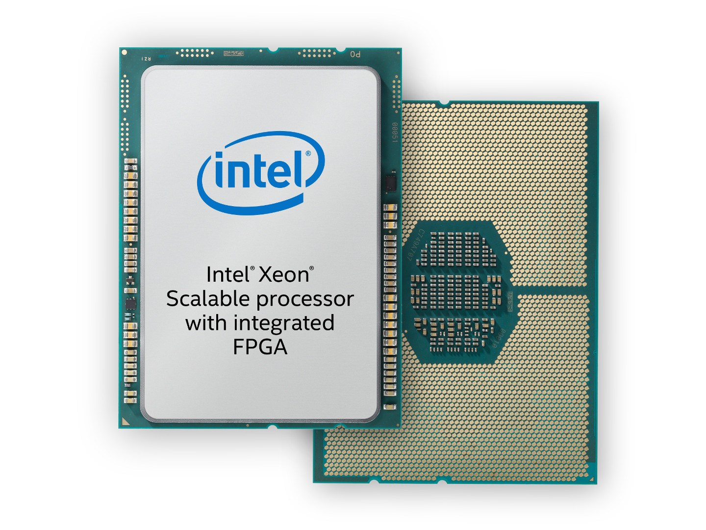
 Image source: Intel Now Intel has finally announced that they are shipping their Xeon 6138P Gold with integrated FPGA accelerator to selected customers.
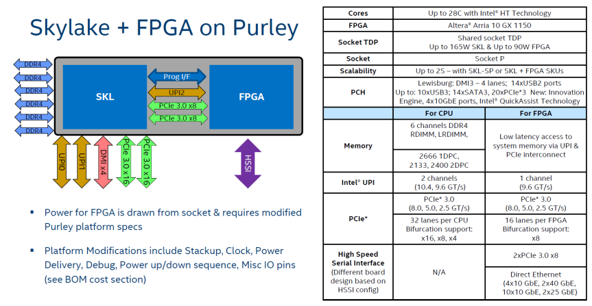 Image Source: Anandtech For more information:


