
Xilinx Virtex-7 V2000T-X690T-HTG700
- Part Number: HTG-V7-PCIE-2000
- Device Support:
- Vendor: HiTech Global Distribution, LLC
- Program Tier: Certified

BTC
Product Description:
Powered by Xilinx Virtex-7 V2000T, V585, or X690T the HTG700 is ideal for ASIC/SOC prototyping, high-performance computing, high-end image processing, PCI Express Gen 2 & 3 development, general purpose FPGA development, and/or applications requiring high speed serial transceivers (up to 12.5Gbps).Key Features and Benefits:
- Scalable via HTG-FMC-FPGA module (with one X980T FPGA) for
- x8 PCI Express Gen2 /Gen 3 edge connectors
- x3 FPGA Mezzanine Connectors (FMC)
- x4 SMA ports (16 SMAs providing 4 Txn/Txp/Rxn/Rxp) clocked by external
- DDR3 SODIMM with support for up to 8GB (shipped with a 1GB module)
- USB to UART bridge
- Configuration through JTAG or Micron G18 Flash
What's Included:
- Reference Designs
- Schematic, User Manual, UCF
- The HTG700 Board
HTG-700: Xilinx Virtex™ -7 PCI Express Development Platform

Powered by Xilinx Virtex-7 V2000T, V585, or X690T the HTG-700 is ideal for ASIC/SOC prototyping, high-performance computing, high-end image processing, PCI Express Gen 2 & 3 development, general purpose FPGA development, and/or applications requiring high speed serial transceivers (up to 12.5Gbps).
Three High Pin Count (HPC) FMC connectors provide access to 480 single-ended I/Os and 24 high-speed Serial Transceivers of the on board Virtex 7 FPGA. Availability of over 100 different off-the-shelf FMC modules extend functionality of the board for variety of different applications.
Eight lane of PCI Express Gen 2 is supported by hard coded controllers inside the Virtex 7 FPGA. The board's layout, performance of the Virtex 7 FPGA fabric, high speed serial transceivers (used for PHY interface), flexible on-board clock/jitter attenuator, along with soft PCI Express Gen 3 IP core allow usage of the board for PCI Express Gen3 applications.
The HTG-700 Virtex 7 FPGA board can be used either in PCI Express mode (plugged into host PC/Server) or stand alone mode (powered by external ATX or wall power supply).


Currently, (08d-10m-2018y), the Bittware cards (CVP-13, XUPVV4) do not require any modifications and will run at full speed out-of-the-box.
If you have a VCU1525 or BCU1525, you should acquire a DC1613A USB dongle to change the core voltage.
This dongle requires modifications to ‘fit’ into the connector on the VCU1525 or BCU1525.
You can make the modifications yourself as described here,
You can purchase buy a fully modified DC1613A from https://shop.fpga.guide.
If you have an Avnet AES-KU040 and you are brave enough to make the complex modifications to run at full hash rate, you can download the modification guide right here (it will be online in a few days).
You can see a video of the modded card On YouTube: Here.
If you have a VCU1525 or BCU1525, we recommend using the TUL Water Block (this water block was designed by TUL, the company that designed the VCU/BCU cards).
The water block can be purchased from https://shop.fpga.guide.
WARNING: Installation of the water block requires a full disassembly of the FPGA card which may void your warranty.
Maximum hash rate (even beyond water-cooling) is achieved by immersion cooling, immersing the card in a non-conductive fluid.
Engineering Fluids makes BC-888 and EC-100 fluids which are non-boiling and easy to use at home. You can buy them here.
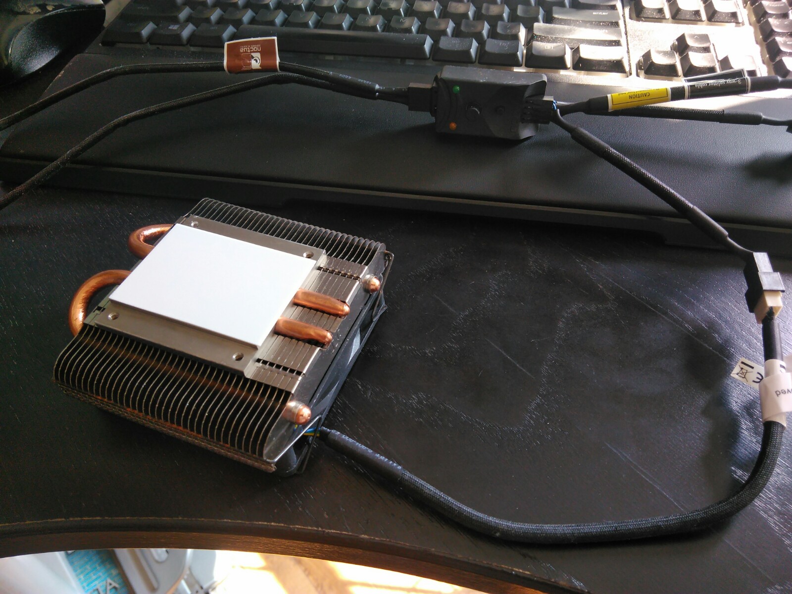
If you have a stock VCU1525, there is a danger of the power regulators failing from overheating, even if the FPGA is very cool.
We recommend a simple modification to cool the power regulators by more than 10C.
The modification is very simple. You need:
Then, you are going to stick the CPU cooler on the back plate of the VCU1525 on this area:
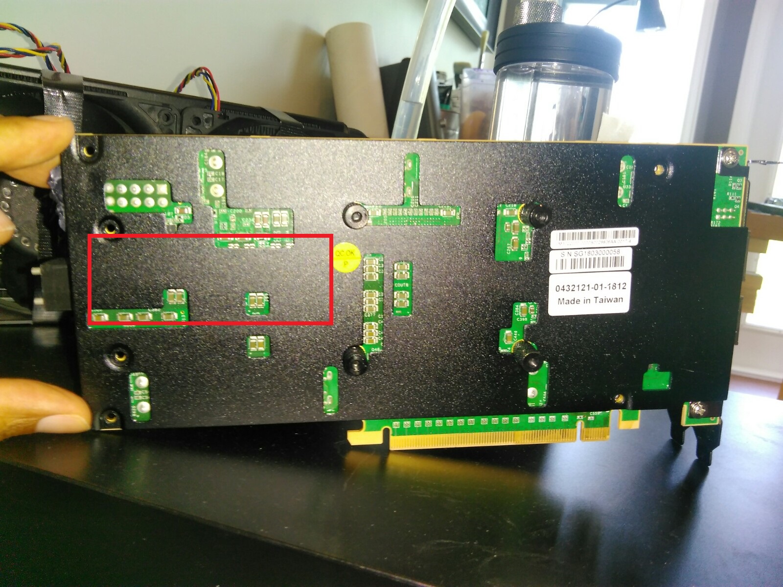
Once done it will look like this:
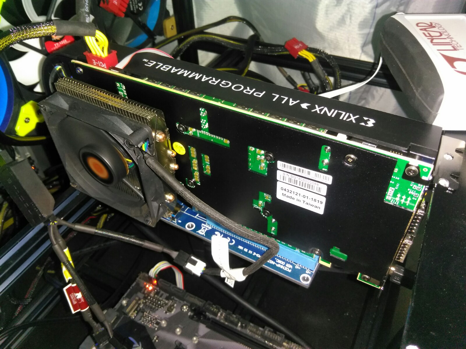
Make sure to connect the fan controller to the power supply and run the fan on maximum speed.
This modification will cool the regulators on the back side of the VCU1525, dropping their temperature by more than 10C and extending the life of your hardware.
This modification is not needed on ‘newer’ versions of the hardware such as the XBB1525 or BCU1525.
OptEdited:
Source-Page:
Grab Bag of FPGA and GPU Software Tools from Intel, Xilinx & NVIDIA
FPGA's as Accelerators:
Hardware:
Tools:
Libraries:
Tools for FPGA + ARM SoC Acceleration Intel:
Xilinx:
Higher Level:
Domain Specific:
Xilinx leverages SDSoC to create an embedded vision stack called reVISION.
Source-Website:
Joerg Schulenburg, Uni-Magdeburg, 2008-2016
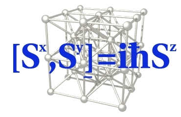
These model systems can for example describe magnetic properties of insulators at very low temperatures (T=0) where the magnetic moments of the particles form entangled quantum states.
The package generates the symmetrized configuration vector, the sparse matrix representing the quantum interactions and computes its eigenvectors and finaly some expectation values for the system.
The first SPINPACK version was based on Nishimori's TITPACK (Lanczos method, no symmetries), but it was early converted to C/C++ and completely rewritten (1994/1995).
Other diagonalization algorithms are implemented too (Lanzcos, 2x2-diagonalization and LAPACK/BLAS for smaller systems). It is able to handle Heisenberg, t-J, and Hubbard-systems up to 64 sites or more using special compiler and CPU features (usually up to 128) or more sites in slower emulation mode (C++ required).
For instance we got the lowest eigenstates for the Heisenberg Hamiltonian on a 40 site square lattice on our machines at 2002. Note that the resources needed for computation grow exponentially with the system size.
The package is written mainly in C to get it running on all unix systems. C++ is only needed for complex eigenvectors and twisted boundary conditions when C has no complex extension. This way the package is very portable.
Parallelization can be done using MPI- and PTHREAD-library. Mixed mode (hybrid mode) is possible, but not always faster than pure MPI (2015). v2.60 has slightly hybrid mode advantage on CPUs supporting hyper-threading.
This will hopefully be improved further. MPI-scaling is tested to work up to 6000 cores, PTHREAD-scaling up to 510 cores but requires careful tuning (scaling 2008-1016).
The program can use all topological symmetries, S(z) symmetry and spin inversion to reduce matrix size. This will reduce the needed computing recources by a linear factor.
Since 2015/2016 CPU vector extensions (SIMD, SSE2, AVX2) are supported to get better performance doing symmetry operations on bit representations of the quantum spins.
The results are very reliable because the package has been used since 1995 in scientific work. Low-latency High-bandwith network and low latency memory is needed to get best performance on large scale clusters.
If you still find some parts written in german or out-of-date documentation send me an email with a short hint where I find this part and I want to rewrite this part as soon as I can.
Please see doc/history.html for latest changes. You can find a documentation about speed in the package or an older version on this spinpack-speed-page.
It also returns a phase factor and the orbit length. It would be a great progress, if the performance of that function could be improved. Ideas are welcome.
One of my motivations is to use FPGAs in 2009 was inspired by the FPGA/VHDL-Compiler.
These are Xilings-tools and are so slow, badly scaling and buggy, that code generation and debugging is really no fun and a much better FPGA toolchain is needed for HPC, but all that is fixed now with updates.
2015-05 I added software benes-network to get gain of AVX2, but it looks like that its still not the maximum available speed (HT shows near 2 factor, bitmask falls out of L1-cache?).
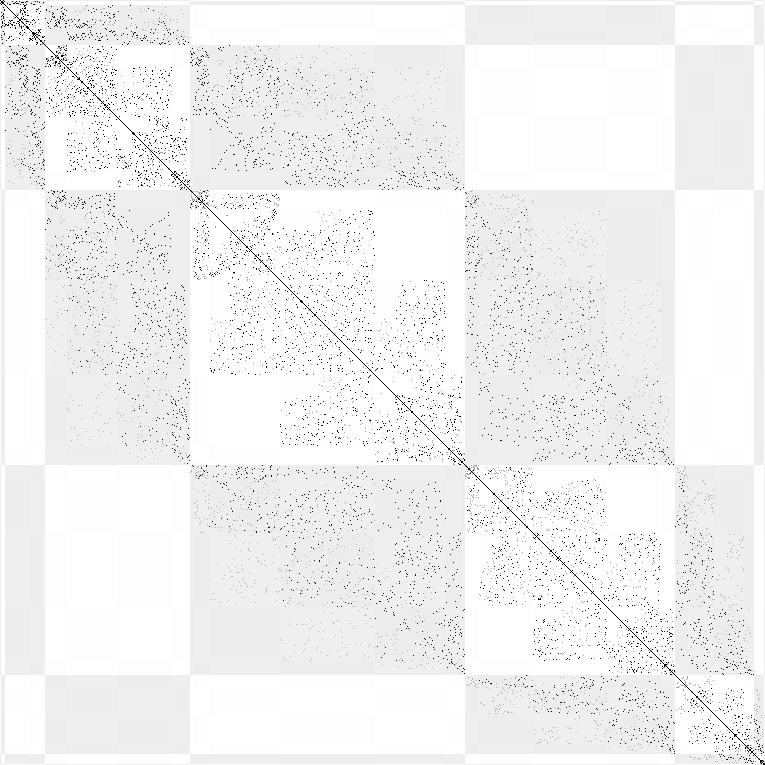
This picture is showing a small sample of a possible Hilbert matrix. The non-zero elements are shown as black pixels (v2.33 Feb2008 kago36z14j2).

This picture is showing a small sample of a possible Hilbert matrix. The non-zero elements are shown as black (J1) and gray (J2) pixels (v2.42 Nov2011 j1j2-chain N=18 Sz=0 k=0). Config space is sorted by J1-Ising-model-Energy to show structures of the matrix. Ising energy ranges are shown as slightly grayed arrays.
Ground state energy scaling for finite size spin=1/2-AFM-chains N=4..40 using up to 300GB memory to store the N=39 sparse matrix and 245 CPU-houres (2011, src=lc.gpl).

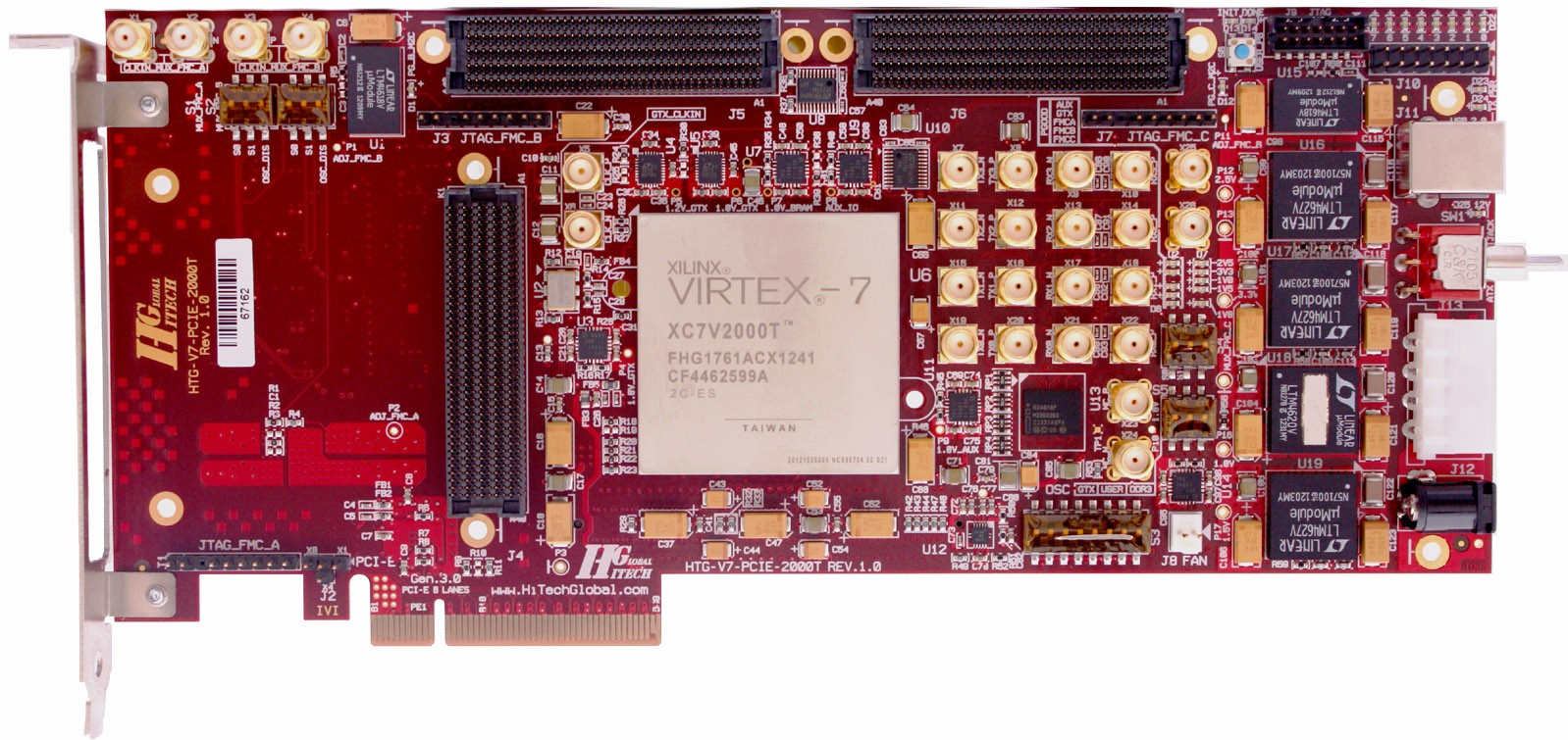
XC7V2000T-x690T_HTG-700: Models
Features:
►Xilinx Virtex-7 V2000T, 585T, or X690T FPGA
►Scalable via HTG-777 FPGA module for providing higher FPGA gate density ► x8 PCI Express Gen2 /Gen 3 edge connectors with jitter cleaner chip - Gen 3: with the -690 option - Gen 2: with the -585 or -2000 option (Gen3 requires soft IP core) ►x3 FPGA Mezzanine Connectors (FMC) - FMC #1: 80 LVDS (160 single-ended) I/Os and 8 GTX (12.5 Gbps) Serial Transceivers - FMC #2: 80 LVDS (160 single-ended) I/Os and 8 GTX (12.5 Gbps) Serial Transceivers - FMC #3: 80 LVDS (160 single-ended) I/Os and 8 GTX (12.5 Gbps) Serial Transceivers. Physical location of this connector allows plug-in FMC daughter cards having easy access to the board through the front panel. ►x4 SMA ports (16 SMAs providing 4 Txn/Txp/Rxn/Rxp) clocked by external pulse generators ►DDR3 SODIMM with support for up to 8GB (shipped with a 2GB module) ►Programmable oscillators (Silicon Labs Si570) for different interfaces ►Configuration through JTAG or Micron G18 Embedded Flash ►USB to UART bridge ►ATX and DC power supplies for PCI Express and Stand Alone operations ►LEDs & Pushbuttons ►Size: 9.5" x 4.25" | Kit Content: Hardware: - HTG-700 board Software: - PCI Express Drivers (evaluation) for Windows & Linux Reference Designs/Demos: - PCI Express Gen3 PIO - 10G & 40G Ethernet (available only if interested in licensing the IP cores) - DDR3 Memory Controller Documents: - User Manual - Schematics (in searchable .pdf format) - User Constraint File (UCF) Ordering information Part Numbers: - HTG-V7-PCIE-2000-2 (populated with V2000T-2 FPGA) Price: Contact Us - HTG-V7-PCIE-690-2 (populated with X690T-2 FPGA) Price: Contact us - HTG-V7-PCIE-690-3 (populated with X690T-3 FPGA) Price: Contact us - HTG-V7-PCIE-585-2 (populated with V585T-2 FPGA) Price: Contact us |
FPGA-(CVP-13, XUPVV4): Hardware Modifications

Currently, (08d-10m-2018y), the Bittware cards (CVP-13, XUPVV4) do not require any modifications and will run at full speed out-of-the-box.
If you have a VCU1525 or BCU1525, you should acquire a DC1613A USB dongle to change the core voltage.
This dongle requires modifications to ‘fit’ into the connector on the VCU1525 or BCU1525.
You can make the modifications yourself as described here,
You can purchase buy a fully modified DC1613A from https://shop.fpga.guide.
If you have an Avnet AES-KU040 and you are brave enough to make the complex modifications to run at full hash rate, you can download the modification guide right here (it will be online in a few days).
You can see a video of the modded card On YouTube: Here.
If you have a VCU1525 or BCU1525, we recommend using the TUL Water Block (this water block was designed by TUL, the company that designed the VCU/BCU cards).
The water block can be purchased from https://shop.fpga.guide.
WARNING: Installation of the water block requires a full disassembly of the FPGA card which may void your warranty.
Maximum hash rate (even beyond water-cooling) is achieved by immersion cooling, immersing the card in a non-conductive fluid.
Engineering Fluids makes BC-888 and EC-100 fluids which are non-boiling and easy to use at home. You can buy them here.
If you have a stock VCU1525, there is a danger of the power regulators failing from overheating, even if the FPGA is very cool.
We recommend a simple modification to cool the power regulators by more than 10C.
The modification is very simple. You need:
- Thermaltake Slim X3 CPU cooler:
- https://www.newegg.com/Product/Product.aspx?Item=N82E16835106152
- Noctua NA-FC1 fan controller or any fan controller/driver:
- https://www.newegg.com/Product/Product.aspx?Item=9SIAADY5SE8250
- Thermal interface tape, any brand will do:
- https://www.digikey.com/product-detail/en/BP100-0.011-00-1010/BER160-ND/307782
Then, you are going to stick the CPU cooler on the back plate of the VCU1525 on this area:
Once done it will look like this:
Make sure to connect the fan controller to the power supply and run the fan on maximum speed.
This modification will cool the regulators on the back side of the VCU1525, dropping their temperature by more than 10C and extending the life of your hardware.
This modification is not needed on ‘newer’ versions of the hardware such as the XBB1525 or BCU1525.
OptEdited:
Source-Page:
Grab Bag of FPGA and GPU Software Tools from Intel, Xilinx & NVIDIA
FPGA's as Accelerators:
- From the Intel® FPGA SDK for OpenCL™ Product Brief available at link.
- "The FPGA is designed to create custom hardware with each instruction being accelerated providing more efficiency use of the hardware than that of the CPU or GPU architecture would allow."
Hardware:
- With Intel, developers can utilize an x86 with a built-in FPGA or connect a card with an Intel or Xilinx FPGA to an x86. This Host + FPGA Acceleration would typically be used in a "server."
- With Intel and Xilinx, developers can also get a chip with an ARM core + FPGA. This FPGA + ARM SoC Acceleration is typically used in embedded systems.
- Developers can also connect a GPU card from Nvidia to an x86 host. Developers can also get an integrated GPU from Intel. Nvidia also provides chips with ARM cores + GPUs.
Tools:
- Intel and Xilinx provide tools to help developers accelerate x86 code execution using an FPGA attached to the x86. They also provide tools to accelerate ARM code execution using an FPGA attached to the ARM.
- Intel, Xilinx and Nvidia all provide OpenCL libraries to access their hardware. These libraries can not interoperate with one another. Intel also provides libraries to support OpenMP and Nvidia provides CUDA for programming their GPUS. Xilinx includes their OpenCL library in an SDK called SDAccel and an SDK called SDSoC. SDAccel is used for x86 + Xilinx FPGA systems, i.e. servers. SDSoC is used for Xilinx chips with ARM + FPGAs, i.e. embedded systems.
Libraries:
- To help developers building computer vision applications, Xilinx provides OpenVX, Caffe, OpenCV and various DNN and CNN libraries in an SDK called reVISION for software running on chips with an ARM+FPGA.
- All of these libraries and many more are available for x86 systems.
- Xilinx also provides neural network inference, HEVC decoders and encoders and SQL data-mover, function accelerator libraries.
Tools for FPGA + ARM SoC Acceleration Intel:
- From link developers can work with ARM SoCs from Intel using:
- ARM DS-5 for debug
- SoC FPGA Embedded Development Suite for embedded software development tools
- Intel® Quartus® Prime Software for working with the programmable logic
- Virtual Platform for simulating the ARM
- SoC Linux for running Linux on the FPGA + ARM SoC
- Higher Level
- Intel® FPGA SDK for OpenCL™ is available for programming the ARM + FPGA chips using OpenCL.
Xilinx:
- Developers can work with ARM SoCs from Xilinx using:
- An SDK for application development and debug
- PetaLinux Tools for Linux development and ARM simulation and
- Vivado for using the PL for working with its FPGA + ARM SoC chips
Higher Level:
- Xilinx provides SDSoC for accelerating ARM applications on the built-in FPGA. Users can program in C and/or C++ and SDSoC will automatically partition the algorithm between the ARM core and the FPGA. Developers can also program using OpenCL and SDSoC will link in an embedded OpenCL library and build the resulting ARM+FPGA system. SDSoC also supports debugging and profiling.
Domain Specific:
Xilinx leverages SDSoC to create an embedded vision stack called reVISION.
Source-Website:
SPINPACK
Author:
Joerg Schulenburg, Uni-Magdeburg, 2008-2016
What is SpinPack?
SPINPACK is a big program package to compute lowest eigenvalues and eigenstates and various expectation values (spin correlations etc) for quantum spin systems.These model systems can for example describe magnetic properties of insulators at very low temperatures (T=0) where the magnetic moments of the particles form entangled quantum states.
The package generates the symmetrized configuration vector, the sparse matrix representing the quantum interactions and computes its eigenvectors and finaly some expectation values for the system.
The first SPINPACK version was based on Nishimori's TITPACK (Lanczos method, no symmetries), but it was early converted to C/C++ and completely rewritten (1994/1995).
Other diagonalization algorithms are implemented too (Lanzcos, 2x2-diagonalization and LAPACK/BLAS for smaller systems). It is able to handle Heisenberg, t-J, and Hubbard-systems up to 64 sites or more using special compiler and CPU features (usually up to 128) or more sites in slower emulation mode (C++ required).
For instance we got the lowest eigenstates for the Heisenberg Hamiltonian on a 40 site square lattice on our machines at 2002. Note that the resources needed for computation grow exponentially with the system size.
The package is written mainly in C to get it running on all unix systems. C++ is only needed for complex eigenvectors and twisted boundary conditions when C has no complex extension. This way the package is very portable.
Parallelization can be done using MPI- and PTHREAD-library. Mixed mode (hybrid mode) is possible, but not always faster than pure MPI (2015). v2.60 has slightly hybrid mode advantage on CPUs supporting hyper-threading.
This will hopefully be improved further. MPI-scaling is tested to work up to 6000 cores, PTHREAD-scaling up to 510 cores but requires careful tuning (scaling 2008-1016).
The program can use all topological symmetries, S(z) symmetry and spin inversion to reduce matrix size. This will reduce the needed computing recources by a linear factor.
Since 2015/2016 CPU vector extensions (SIMD, SSE2, AVX2) are supported to get better performance doing symmetry operations on bit representations of the quantum spins.
The results are very reliable because the package has been used since 1995 in scientific work. Low-latency High-bandwith network and low latency memory is needed to get best performance on large scale clusters.
News:
- Groundstate of the S=1/2 Heisenberg AFM on a N=42 kagome biggest sub-matrix computed (Sz=1 k=Pi/7 size=36.7e9, nnz=41.59, v2.56 cplx8, using partly non-blocking hybrid code on supermuc.phase1 10400cores(650 nodes, 2 tasks/node, 8cores/task, 2hyperthreads/core, 4h), matrix_storage=0.964e6nz/s/core SpMV=6.58e6nz/s/core Feb2017)
- Groundstate of the S=1/2 Heisenberg AFM on a N=42 linear chain computed (E0/Nw=-0.22180752, Hsize = 3.2e9, v2.38, Jan2009) using 900 Nodes of a SiCortex SC5832 700MHz 4GB RAM/Node (320min).
Update: N=41 Hsize = 6.6e9, E0/Nw=-0.22107343 16*(16cores+256GB+IB)*32h matrix stored, v2.41 Oct2011). - Groundstate of the S=1/2 Heisenberg AFM on a N=42 square lattice computed (E0 = -28.43433834, Hsize = 1602437797, ((7,3),(0,6)), v2.34, Apr2008) using 23 Nodes a 2*DualOpteron-2.2GHz 4GB RAM via 1Gb-eth (92Cores usage=80%, ca.60GB RAM, 80MB/s BW, 250h/100It).
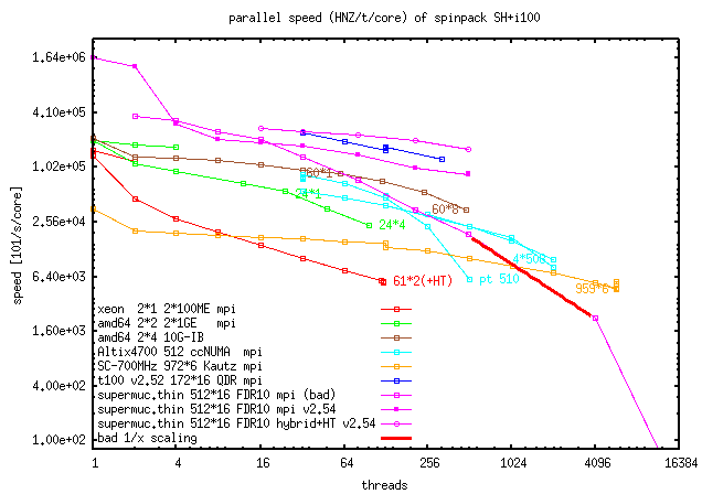
- Program is ready for cluster (MPI and Pthread can be used at the same time, see the performance graphic) and can again use memory as storage media for performance measurement (Dec07).
- Groundstate of the S=1/2 Heisenberg AFM on a N=40 square lattice computed (E0 = -27.09485025, Hsize = 430909650, v1.9.3, Jan2002).
- Groundstate of the S=1/2 J1-J2-Heisenberg AFM on a N=40 square lattice J2=0.5, zero-momentum space: E0= -19.96304839, Hsize = 430909650 (15GB memory, 185GB disk, v2.23, 60 iterations, 210h, Altix-330 IA64-1.5GHz, 2 CPUs, GCC-3.3, Jan06)
- Groundstate of the S=1/2 Heisenberg AFM on a N=39 triangular lattice computed (E0 = -21.7060606, Hsize = 589088346, v2.19, Jan2004).
- Largest complex Matrix: Hsize=1.2e9 (26GB memory, 288GB disk, v2.19 Jul2003), 90 iterations: 374h alpha-1GHz (with limited disk data rate, 4 CPUs, til4_36)
- Largest real Matrix: Hsize=1.3e9 (18GB memory, 259GB disk, v2.21 Apr2004), 90 iterations: real=40h cpu=127h sys=9% alpha-1.15GHz (8 CPUs, til9_42z7)
Download:
Verify download using:gpg --verify spinpack-2.55.tgz.asc spinpack-2.54.tgz- spinpack.tgz experimental developper version (may have bug fixes, new features or speed improvements, see doc/history.html)
- spinpack-2.56c.tgz 2.57 backport fixes, above 2048*16threads, FTLM-random-fix, see doc/history
- spinpack-2.56.tgz better hybrid MPI-scaling above 1000 tasks, tested on kagome42_sym14_sz13..6, pgp-sign, updated 2017-02-23, see doc/history, still blocking MPI only)
- spinpack-2.55.tgz better MPI-scaling above 1000 tasks, tested on kagome42_sym14_sz13..8..1, pgp-sign, updated 2017-02-21, see doc/history)
- spinpack-2.52.tgz OpenMP-support (implemented as pthread-emulation), but weak mixed code speed, pgp-sign, Dec16)
- spinpack-2.51.tgz g++6-adaptions (gcc6.2 compile-errors/warnings fixed, pgp-sign, Sep16)
- spinpack-2.50d.tgz SIMD-support (SSE2,AVX2), lot of bug-fixes (Jan16+fixFeb16+fixMar16b+c+fixApr16d))
- spinpack-2.49.tgz mostly bug-fixes (Mar15) (updated Mar15,12, buggy bfly-bench, NN>32 32bit-compile-error.patch, see experimental version above)
- spinpack-2.48.tgz test-version (v2.48pre Feb14 new features, +tUfixMay14 +chkptFixDez14 +2ndrunFixJan15)
- spinpack-2.47.tgz bug fixes (see doc/history.html, bug fixes of 2.45-2.46) (version 2014/02/14, 1MB, gpg-signatur)
- spinpack-2.44.tgz (see doc/history.html, known bugs) (version 2013/01/23 + fix May13,May14 2.44c, 1MB, gpg-signatur)
- spinpack-2.43.tgz +checkpointing (see doc/history.html) (version 2012/05/23, 1MB, gpg-signatur)
- spinpack-2.42.tgz ns.mpi-speed++ (see doc/history.html) (version 2012/05/07, 1MB, gpg-signatur)
- spinpack-2.41.tgz mpi-speed++,doc++ (see doc/history.html) (version 2011/10/24 + backport-fix 2015-09-23, 1MB, gpg-signatur)
- spinpack-2.40.tgz bug fixes (see doc/history.html) (version 2009/11/26, 890kB, gpg-signatur)
- spinpack-2.39.tgz new option -m, new lattice (doc/history.html) (version 2009/04/20, 849kB, gpg-signatur)
- spinpack-2.38.tgz MPI-fixes (doc/history.html) (version 2009/02/11, 849kB, gpg-signatur)
- spinpack-2.36.tgz MPI-tuned (doc/history.html) (version 2008/08/04, 802kB, gpg-signatur)
- spinpack-2.35.tgz IA64-tuned (doc/history.html) (version 2008/07/21, 796kB, gpg-signatur)
- spinpack-2.34.tgz bugs fixed for MPI (doc/history.html) (version 2008/04/23, 770kB, gpg-signatur)
- spinpack-2.33.tgz bugs fixed for MPI (doc/history.html) (version 2008/03/16, 620kB, gpg-signatur)
- spinpack-2.32.tgz bug fixed (doc/history.html) (version 2008/02/19, 544kB, gpg-signatur)
- spinpack-2.31.tgz MPI works and scales (version 2007/12/14, 544kB, gpg-signatur)
- spinpack-2.26.tgz code simplified and partly speedup, prepare for FPGA and MPI (version 07/02/27, gpg-signatur)
- spinpack-2.15.tgz see doc/history.tex (updated 2003/01/20)
Installation:
- gunzip -c spinpack-xxx.tgz | tar -xf - # xxx is the version number
- cd spinpack; ./configure --mpt
- make test # to test the package and create exe path
- # edit src/config.h exe/daten.def for your needs (see models/*.c)
- make
- cd exe; ./spin
Documentation:
The documentation is available in the doc-path. Most parts of the documentation are rewritten in english now.If you still find some parts written in german or out-of-date documentation send me an email with a short hint where I find this part and I want to rewrite this part as soon as I can.
Please see doc/history.html for latest changes. You can find a documentation about speed in the package or an older version on this spinpack-speed-page.
Most Important Function:
The most time consuming important function isb_smallest in hilbert.c. This function computes the representator of a set of symmetric spin configurations (bit pattern) from a member of this set.It also returns a phase factor and the orbit length. It would be a great progress, if the performance of that function could be improved. Ideas are welcome.
One of my motivations is to use FPGAs in 2009 was inspired by the FPGA/VHDL-Compiler.
These are Xilings-tools and are so slow, badly scaling and buggy, that code generation and debugging is really no fun and a much better FPGA toolchain is needed for HPC, but all that is fixed now with updates.
2015-05 I added software benes-network to get gain of AVX2, but it looks like that its still not the maximum available speed (HT shows near 2 factor, bitmask falls out of L1-cache?).
Examples for open access
Please use these data for your work or verify my data. Questions and corrections are welcome. If you miss data or explanations here, please send a note to me.- s=1/2 Heisenberg model square lattice (finite size extrapolation: gnuplot data, gnuplot script)
- s=1/2 Heisenberg model triangular lattice (finite size extrapolation: gnuplot data, gnuplot script)
- s=1/2 Heisenberg model kagome lattice (finite size extrapolation: gnuplot script, data included)
Frequently asked questions (FAQ):
 Q: I try to diagonalize a 4-spin system, but I do not get the full spectrum. Why?
 A: Spinpack is designed to handle big systems. Therefore it uses as much
    symmetries as it can. The very small 4-spin system has a very special
    symmetry which makes it equivalent to a 2-spin system build by two s=1 spins.
    Spinpack uses this symmetry automatically to give you the possibility
    to emulate s=1 (or s=3/2,etc) spin systems by pairs of s=1/2 spins.
    If you want to switch this off, edit src/config.h and change
    CONFIG_S1SYM to CONFIG_NOS1SYM.
This picture is showing a small sample of a possible Hilbert matrix. The non-zero elements are shown as black pixels (v2.33 Feb2008 kago36z14j2).
This picture is showing a small sample of a possible Hilbert matrix. The non-zero elements are shown as black (J1) and gray (J2) pixels (v2.42 Nov2011 j1j2-chain N=18 Sz=0 k=0). Config space is sorted by J1-Ising-model-Energy to show structures of the matrix. Ising energy ranges are shown as slightly grayed arrays.
Ground state energy scaling for finite size spin=1/2-AFM-chains N=4..40 using up to 300GB memory to store the N=39 sparse matrix and 245 CPU-houres (2011, src=lc.gpl).
Author: Joerg Schulenburg, Uni-Magdeburg, 2008-2016
XC7V2000T-x690T_HTG-700: Models


