CryptoURANUS Economics

Anti-AdBlocker

Sunday, July 21, 2019

Monero-Coin [XMR]: Cryptocurrency


Monero-Coin [XMR]:


About Monero:

Monero is the 9th cryptocurrency based on market capitalization.

Monero is designed to be private, secure and untraceable cryptocurrency.

Official ticker-symbol of Monero is XMR.

Monero Team is motivated building Monero into a primary cryptocurrency leader on the international market, larger than Bitcoin, and always easier to buy and trade for everyone equally and just not the wealthy...

Read more about this currencies here: Forked Monero Coins...


Introduction:


Monero takes decentralization into a prime-directive of function.

“Governments monitor Monero and rarely intervene unless you appear criminal in activity”.

Monero is the gold standard of privacy among cryptocurrencies.
Monero’s prime-directive is being untraceable digital currency to lower hackers, but not upper government, unavoidable.

Monero obfuscates all information on the blockchain with cryptography.

All Monero activities of transaction amounts, senders’ and receivers’ addresses they are all hidden.

The Prime-Directive is Monero default.

No Monero user can undermine the privacy of other users.

Monero have been In development since April 2014.

Monero’s core team included only seven people.

Monero is an open source project.

Monero had many people add to it over time-line of years durring it's existence since April-2014.

Monero didn’t have any ICO (Initial Coin Offering) and wasn’t pre-mined.


The emission of Monero is divided into two phases:

  1. The main emission includes about 18 million coins which will be mined by May 2020. 
  2. Afterwards, the tail emission kicks in, locking the reward rate at 0.6 XMR per 2-minute block, leaving the inflation rate at around 1% a year.

In the near future, Monero inends adamantly to further increase its security by reaching the milestone dubbed the Kovri project.

Kovri aims to create a protected overlay-network across the internet, allowing users to effectively hide their geographical location and internet IP address from high-range, mid-range, and to low-level hackers.

It is based on the open-source decentralized and encrypted communication protocol I2P (somewhat similar to TOR and Onion routing, but far more efficient).

Those Who Have Influenced Monero: 


Riccardo Spagni:
One of the seven core developers and one of the two who publicly revealed their identity.  Riccardo has an extensive business experience and understanding of cryptocurrencies, cryptography and software development.

Francisco "ArticMine" CabaƱas:
Has been researching and investing in cryptocurrencies since 2011. He holds a PhD in Physics, has an extensive business and non-profit experience and focuses on the economic, social, regulatory and long-term viability aspects of cryptocurrencies.

Technology and Fungibility:


The word, fungibility means that any two currency units of the same size can be mutually substituted for each other.

Monero is fungible, because the currency provides no way to link transactions together or trace the history of any particular XMR Monero-Coin.

This is a stark contrast to Bitcoin and most other cryptocurrencies with an open blockchain.

Some large Bitcoin companies were blocking, suspending, or closing accounts that have received Bitcoins used in online gambling or illegal activities without the receiving party’s knowledge.

Monero has been built specifically to avoid this problem by having transactions private.

Stealth Addresses (Recipient Privacy):


Monero's stealth addresses are random one-time addresses created for every transaction on behalf of the recipient of XMR, each and every time, creating privacy for all traders and buyers.

While the recipient has a single public address, every transaction goes to a different unique address on the blockchain and transactions thus cannot be linked to the receiver.

Ring signature (Sender Privacy):


Ring signature is a digital signature which uses a group of people to sign on a transaction.

It is nearly impossible to determine which of the group members’ key was used for the signature.

Ring Confidential Transactions (Amount obfuscation):


There was a modification to the original CryptoNote protocol implemented by January 2017, which hides the amount sent in a transaction. Based on Confidential Transactions from Bitcoin but used with ring signatures.

Advantages:

  • Complete privacy and an anonymous blockchain.
  • Untraceability of the coin.
  • Hidden amounts of transactions.
  • Scheduled hardforks.
  • CryptoNight PoW, an ASIC-resistant algorithm.
  • Dynamic blocksize.
  • Dynamic fees.
  • Disadvantages.
  • Rate of Blockchain growth.
  • Smaller and slower adoption of the crypto.
  • Whitepaper.

Monero does not have a whitepaper, the currency's technical solution is based on CryptoNote.

CryptoNote's whitepaper examines Bitcoin's POW algorithm, hard-coded constants, irregular emission and other shortcomings of Bitcoin and presents how CryptoNote is tackling these with the egalitarian “one-CPU-one-vote” CryptoNight algorithm.

Real examples of use:


Monero has fewer uses compared to Bitcoin and bitcoin-based currencies.

There aren’t any Monero ATMs at the moment, it will take some time for Monero to be integrated into hardware wallets, but the developers community is already working on it.

The most prominent use of Monero is with drug dealers, mafia's, and other black-project agencies on the darknet.

All governments around the world are spreading Monero among ordinary people that just don´t want to be spied-on, buy excessive use of this currency in their black projects...


What is Monero?
Monero is the leading cryptocurrency within the privacy alt.coin cryptocurrencies.

All transactions on the blockchain are obfuscated by default

Monero is fungible - individual coins cannot be tainted

Decentralized development by cryptography experts with exception to quantum entanglement sentient technologies.


The Complete Guide to Monero Cryptocurrency:
monero

Monero, Regards Bitcoin and Ethereum are literally hundreds of other coins, and each of them claim to offer different improvements on Bitcoin and this does never will manner in any extreme case!

Why? They offer no privacy from the big banks and their agency puppets from putting you in prison.

Some have cheaper transactions, some may be faster but, Monero is one of the most and completely anonymous.

That’s right!

The high-tech cryptography programmers, the sender, receiver, and the amount of Monero sent is impossible to view by anyone else.

Monero is founded on this unique technique of escape and evasion of international bank ibdustry.

Monero’s have strong cryptography and privacy

The History of Monero:


To trace the historic origins of Monero, we need to look at a different cryptocurrency – Bytecoin.

Bytecoin was launched in the summer of 2012.

It was the first digital currency that was written using a technology called CryptoNote.

CryptoNote today is the backbone of most of the privacy-based cryptocurrencies that exist and this includes Monero.

The privacy of CryptoNote coins is ensured by grouping public keys together.

By combining several keys in a single transaction, it’s impossible to tell who sent it!

The use of these “ring signatures” to sign transactions provides the anonymity of the CryptoNote technology.

Bytecoin is an effort at anonymous cryptocurrency. There are issues with bytecoin initial distribution. There was 80% of these coins were already in existence.

This lead a group of seven developers to fork the Bytecoin blockchain and the new currency would be known as Bitmonero. This was eventually shortened to simply Monero which is Esperanto for “coin”.

Of the seven developers who originally created Monero, five of them decided that they would keep their identities secret. Only two of these Monero developers are known about – Riccardo Spagni (the main developer today) and David Latapie. Riccardo Spagni is also known by the nickname “Fluffypony”.

What Makes Monero Different?

Monero is an an open-source project that is entirely permission-less and private.

There is no authority that can stop you from using Monero cryptocurrency, not ever, not one on Earth.

This means that those without access to modern banking facilities can take part in a digital economy in the way they never could before privately, securely, and without being traced.

All they need is an internet connection and a device to connect to it.

There are literally millions of people around the world that lack access to banking facilities but have smartphones and local Wi-Fi hotspots.

India is a prime example of a country with many of these “unbanked” citizen activities.


Privacy:

The main thing that gives Monero value is its extreme privacy features.

No one can link you to a Monero cryptocurrency transaction.

This makes it a favorite currency for those who are concerned with privacy for a variety of reasons.

Not all these reasons will be illegal although some obviously will be.


Fungibility:
Another very important feature of the Monero cryptocurrency related to privacy features is entirely fungible.

It’s possible to track Bitcoin transactions from one user to another. Depending on how the user uses Bitcoin, you might not be able to tell their identity, but you can follow each Bitcoin from address to address.

The advanced privacy features of Monero allows no-one to see which transactions each coin was actually involved in.

It would be entirely impossible to link a single Monero coin to a past crime, but other non-privacy coins are easily tracable. There is no transaction history associated with any Monero coins. This means they are fungible!
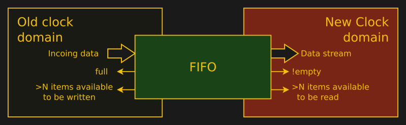
Dynamic Scalability:
Monero improved Bitcoin by scalability.

The Monero scalability just means how well the network can grow in relation to demand.

Blockchain-based cryptocurrencies are by definition limited in size.

For much of its past, Bitcoin has had a 1MB block-size limit.

This means that only 1MB of transaction data can fit into each of the blocks that are mined every 10 minutes on the Bitcoin network.

Unfortunately, when there are many users trying to make transactions at the same time using Bitcoin, the blockchain gets filled with transaction data.

Those transactions that can’t fit into a block must wait for a miner to include them.

Since miners prefer to include transactions with the largest fees attached, if the network is very busy, it encourages people to increase the fees to get their transactions included.

This is what happened in the Spring of 2017 to the Bitcoin blockchain. Some transactions were actually requiring a $30+ fee just to be validated!

Monero is different.

There is no “pre-set” block size limit.

Whilst this does allow for more transaction data in each block, there is a downside – spammers can fill the blockchain with transactions and this makes huge blocks.

So, The Monero developers introduced a block reward-penalty system.

The median size of the last 100 blocks is taken. If the new block that the miners are working on exceeds the median of the previous hundred blocks, the block reward is reduced.

This discourages spam transactions since miners won’t mine blocks that are subject to such a large penalty if it’s no longer profitable for them to do so.
   

The block reward will never drop below 0.3 XMR, making Monero a disinflationary currency: the inflation will be roughly 1% in 2022 and go down forever, but the nominal inflation will stay at 0.3 XMR per minute. This means that there will always be an incentive for miners to mine Monero and thus keeping the blockchain secure, with or without a fee market.
ASIC Resistance:
Another common issue with Bitcoin is that mining the network is now only profitable using specialized mining equipment.

These systems use components known as Application Specific Integrated Circuit chips, (ASIC).

These mining machines are very expensive and this means that only the richest can set up mining operations.

Monero does not conform and allows anyone with a computer to participate.

It uses an alternate hashing algorithm in opposition to Bitcoin called CryptoNight.

CryptoNight uses a lot of advanced features to make the production of ASIC chips suitable for mining Monero is unprofitable and unnecessary.

The specifics of this algorithm is a little complex for introduction to the Monero currency, and all need mining Monero is by using both CPUs and GPUs of any personal computer, workstation, data-center, and-or server.

With this algorithm the currency primarily decentralized than Bitcoin and-or any-other cryptocurrency available today.

Multiple Keys:
Monero uses a different set of system keys in opposition to Bitcoin and Ethereum.

In these currencies, there is just one pair of keys making Bitcoin and Bitcoin variants traceable and-or more easily hackable; a public key and a private key.

Monero uses a public view key, a private view key, and both public and private spend key.
  • A one uses only stealth public address is generated by the public view key.
  • For checking the blockchain and verifying that funds have been received, a private view key is needed.
  • To verify the signature on a transaction requires a public spend key.
  • Private spend keys are used to create outgoing transactions.
Monero and Supply:
In opposition to Bitcoin, Monero has no fixed number of tokens that will ever be mined.

The currency is slightly inflationary.

There will initially be 18.5 million coins, following this the supply will increase approximately by around 0.87% in each year.

This percentage lowers each year. It’s estimated that it will take 117 years to reach double the initial distribution.

For this figure to double again it will take 234 years. At the time of writing (May 18, 2018) there are 16,040,000 just in case you find the fountain of youth and live a very long life.

Monero and a Wider Cryptocurrency Market:
The current price for a single XMR coin is to-date: July-21st-2019 is $84.25 at present.

The currency is the 12th most popular in terms of total market capitalization.

Below, is included a graph of the Monero coin’s performance since it was launched.

As you can see, like most cryptocurrencies, the value spiked around January 2018 and has fallen back quite a bit since its all-time high of $480.

 
How to Store Monero:
Storing Monero used to be quite a struggle.

You would need to run the wallet using command lines or a hard-wallet.

Although this made you feel like you were hacking into some secret government database, it wasn’t exactly user-friendly!

Fortunately, there is now a much easier way to store Monero!
First head to www.mymonero.com.
  • Click “create account”.
How to create an account on Monero website
  • Read and understand the page about the importance of securely storing your private key login information.
  • Write down your private login key.
  • Type the private login key into the box below the key. This is to check you actually did make a note of it. The one pictured below is an empty account. You can check it by all means but you will be wasting your time!
Monero Private Login Key
You’ve just created your first Monero wallet. Lets assume you want to put some XMR coins in the wallet. Outlined below are steps to do this:

Storing XMR

  • Make a note of the address at the top of the Account overview screen, OK?
Monero
  • Go to the exchange account that you want to send Monero from.
  • Enter the address you just made a note of under the exchange’s withdrawal section.
  • Follow the on-screen prompts to complete the withdrawal. Some exchanges might ask you to confirm that you are making the withdrawal by clicking a link in an email.
  • If you’re receiving Monero from a friend, simply send them the address and they should know what to do with it!
If you want to send Monero from your wallet, I have provided the instructions to do this as well.

Sending XMR

  • First, click “send”.
Monero
  • Enter the address that you wish to send Monero to. You will get this from either an exchange, a contact (friend or colleague, etc), or any service that accepts Monero as a payment option.
  • Type the amount you want to send in the box labeled “amount”.
  • Select how private you want the transaction to be. The greater the “ring size” the higher the transaction fee will have to be.
  • Hit “send payment”.
That’s it, that’s all there is to using the MyMonero wallet. I think you’ll agree it’s much easier than wrestling with the command prompt wallet. However, you won’t win many elite hacker points for using MyMonero!

The Advantages and Disadvantages of Monero

PROs
One of the most private cryptocurrencies to date:21st-July-2019.
Transactions are impossible to link to a person.
Transactions are impossible to trace.
The blockchain doesn’t have a limit as Bitcoin and other cryptocurrencies.
The dynamic scalability means fees are not huge even if used a lot.
It’s possible to choose who can see your transactions.
[For example, if you wanted to prove your ownership of a certain amount of Monero for tax purposes, you can share your private view key with your countries tax authority. This makes it less likely that regulators will try to ban Monero.]
A great team of committed developers works on the project.
You can mine Monero from a local node avoiding a remote pool.

CONs
Despite being ASIC resistant, there is centralization of remote miners on Monero. Roughly 43% of the hash rate is controlled by just three remote server pools.
There are only few high tech wallets that have been developed for Monero.
To store Monero in a way that is properly secure is much tougher than most other cryptocurrencies. This might be why it hasn’t been more widely adopted by the wider community.
Monero is not based on Bitcoin, and it is harder to develop applications that interact with its blockchain.
Monero In The Future:
On Planet Earth, a world whereby absolutely nothing seems to offer genuine privacy anymore, there is certainly a call for such privacy-focused currencies as Monero.

Listed are both legal example where private money was a good thing earlier, as well as an illegal but morally defensible ones equally.

Monero allows people to transact nearly in an instant across the world without any need for permission from any authority.

In countries with open publicized oppressive governments, this could be used as a very powerful tool in the pursuit of freedom.

Most wealthy individuals are criminals and also appreciate the privacy features of Monero.

Most wealthy individuals are criminals dark-web market places whereby they accessed an array of drugs, weapons, and other criminal items that thousandaires, and millionaires alike love partaking in.

Monero has quickly found a place as the currency of choice on these illicit websites.

Monero has also been used by governments such as North Korea’s to get around international sanctions.

Monero is used for black-ops by governments. Monero is used by the wealthy for child pornography, wealthy drug dealers, and international terrorist organizations and human traffickers.

The non-wealthy citizens of earth that are not criminals use Monero for privacy purposes so the wealthy do not steal their money.

Remember, those millionaire who steal cryptocurrency for drugs, for child-pornography, for raping small pubecent children, kidnapping small teenage children then drinking their blood and cannabalizing them, and that common millionaire pass-time of animal sex with Monero coins is horrible.

Do not do as the evil wealthy people do, OK? :) 

Since you are a common good decent moral and ethical citizen who is not a demonic prick of a millionaire then Monero is for you.


Conclusion
Before I end this blogger post, let us have a recap. You should have learn:
  • What is Monero?
  • Monero’s history.
  • What Monero is useful for.
  • A little about how it achieves its privacy and anonymity.
  • How to set up and use a Monero wallet in the easiest (although not most secure) way.
  • How Monero differs from Bitcoin.
  • The current and past Monero value.
  • The advantages and disadvantages of using Monero.
  • The future of Monero.
I hope you found this guide to Monero interesting and educational! Monero has the potential to become a very powerful tool of resistance, as well as a handy payment method for both legal and illegal goods and services.
With all your new-found knowledge, what do you think about Monero? Does this project have a future, or will the governments of the world try to entirely ban it? I’d love to hear your thoughts on the subject!

This is the link to Monero Offficial Website.


Heads UP Monero News:

Torrent website The Pirate Bay is doubling down on its plan to use visitors' processing power to mine crypto.

In a disclaimer recently added to the bottom of its homepage, the website said that "by entering TPB you agree to [monero] being mined using your CPU. If you don't agree please leave now or install an adBlocker."

That message comes months after the site's administrators wrote in a September blog post that they were testing a monero Javascript miner in an effort to, as they put it, "get rid of all the ads."

It was a controversial effort launched by an equally controversial website, which has drawn the ire of numerous national governments for its role in facilitating file-sharing online.

Many TPB visitors cried foul as much of their computing power was harnessed for mining XMR. Bleeping Computer reported last October that Pirate Bay had brought back the feature.

The TPB torrent site's new approach represents a kind of so-called "cryptojacking" that is voluntary in nature.

Indeed, other organizations, including the United Nations Children's Fund (UNICEF), have turned to the Coinhive open-source software as a source of revenue (though in that case, the revenues are destined for philanthropic causes).

Other instances of "cryptojacking" have been far more malicious in nature, including a wide-ranging attack this spring which targeted websites running the Drupal content management system.


This is GitHug Source Link Here.

Cloning the repository

Clone recursively to pull-in needed submodule(s):
$ git clone --recursive https://github.com/monero-project/monero
If you already have a repo cloned, initialize and update:
$ cd monero && git submodule init && git submodule update

Build instructions

Monero uses the CMake build system and a top-level Makefile that invokes cmake commands as needed.

On Linux and OS X

  • Install the dependencies
  • Change to the root of the source code directory, change to the most recent release branch, and build:
      cd monero
      git checkout v0.13.0.0
      make
    
    Optional: If your machine has several cores and enough memory, enable parallel build by running make -j<number of threads> instead of make. For this to be worthwhile, the machine should have one core and about 2GB of RAM available per thread.
    Note: If cmake can not find zmq.hpp file on OS X, installing zmq.hpp from https://github.com/zeromq/cppzmq to /usr/local/include should fix that error.
    Note: The instructions above will compile the most stable release of the Monero software. If you would like to use and test the most recent software, use git checkout master. The master branch may contain updates that are both unstable and incompatible with release software, though testing is always encouraged.
  • The resulting executables can be found in build/release/bin
  • Add PATH="$PATH:$HOME/monero/build/release/bin" to .profile
  • Run Monero with monerod --detach
  • Optional: build and run the test suite to verify the binaries:
      make release-test
    
    NOTE: core_tests test may take a few hours to complete.
  • Optional: to build binaries suitable for debugging:
       make debug
    
  • Optional: to build statically-linked binaries:
       make release-static
    
Dependencies need to be built with -fPIC. Static libraries usually aren't, so you may have to build them yourself with -fPIC. Refer to their documentation for how to build them.
  • Optional: build documentation in doc/html (omit HAVE_DOT=YES if graphviz is not installed):
      HAVE_DOT=YES doxygen Doxyfile
    

Saturday, July 20, 2019

Account-Accounting: Cryptocurrency


Account/Accounting method/Accounts Receivable Turnover: defined in CryptoCurrency


An Account in Cryptocurrency; is access to a computer, website or software that allows users to access the tools located within within their membership account.

Access is usually gained through a username and password, but with cryptocurrencies, it is strongly directed to be accessed with private key(s).


Accounting Method, and What is an accounting method?


      An accounting method is the set of guidelines and rules businesses use to keep financial records and prepare financial reports for the purpose of taxation.

Deeper definition:

The accounting method helps in reporting income and expenses for the purpose of taxation, as well as decision-making by the management of a business. Taxpayers are required by the IRS to have an accurate method of showing their income and expenses. They are also obliged to ensure consistency in their accounting method of choice every year. The selection of the accounting method is usually based on tax minimization and regulation strategies.

There are two primary accounting methods used in record keeping: accrual basis and cash basis. Under the cash basis, expenses and incomes are recognized according to real-time cash flow. Income is recorded once the funds are received, as opposed to when they are earned. Likewise, expenses are recorded when they are paid, and not when they are incurred. This method allows for deferment of taxable income, which can be achieved through delayed billing that ensures payment does not come in the current year. Payments can also be accelerated by immediately paying bills that are received before the due date.
Companies that use the accrual basis of accounting recognize income and expenses as soon as they are earned or incurred, even if the cash associated with the transactions has not been transferred. In this basis, revenue is recorded when earned, even before it has been received. Likewise, expenses are recorded when incurred, regardless of when payments are made.

Accounting method example:

Company A has an annual rent of $12,000. The company has a policy of paying this amount at the beginning of the year. If the firm records the transaction on a cash basis, the rent expense will be recorded in January as $12,000. On the other hand, if the firm uses the accrual basis, the account entry for rent in January will be $1,000 ($12,000 divided by 12 months).


Accounts Receivable Turnover and What is Accounts Receivable Turnover?

Accounts receivable turnover is the number of times per year that a business collects its average accounts receivable. Accountants and analysts use accounts receivable turnover to measure how efficiently companies collect on the credit that they provide their customers.

Deeper definition:


Accounts receivable turnover is described as a ratio of average accounts receivable for a period divided by the net credit sales for that same period. This ratio gives the business a solid idea of how efficiently it collects on debts owed toward credit it extended, with a lower number showing higher efficiency.
To calculate the accounts receivable turnover, start by adding the beginning and ending accounts receivable and divide it by 2 to calculate the average accounts receivable for the period. Take that figure and divide it into the net credit sales for the year for the average accounts receivable turnover. The formula looks like the following:
  • Step 1: Beginning accounts receivable + ending accounts receivable / 2 = net accounts receivable
  • Step 2: Net credit sales / accounts receivable = accounts receivable turnover
Do you owe on unpaid credit? Consider a balance-transfer credit card to help manage your debt.

Accounts receivable turnover example:

Corporation A has a beginning accounts receivable of $125,000 and an ending accounts receivable of $235,000 and a net credit sales of $2.8 million, the formula would look like this:
  • Step 1: $125,000 + $235,000 = $360,000 / 2 = $180,000
  • Step 2: $2,800,000 / $180,000 = 15.55
Corporation A has an accounts receivable turnover of 15.55. Company C, its biggest competitor has an accounts receivable turnover of 21, while Corporation B has an accounts receivable turnover of 10. Based on these numbers, Corporation B has the strongest collections.


Hardware-FPGA Offloading-CPU-GPU: Cryptocurrency


Hardware-FPGA Offloading-CPU-GPU


Hardware-FPGA Offloading-CPU-GPU: As an industry standard preferred TCP/IP, CPU, GPU hardware offloading card is the Xilinx XCVU440 chip on the HTG-840 Card. Their is no other work-engine on Virtex-7 UltraScale+ Xilinx market. Their is no other more powerful FPGA chip in the Virtex-7 UltraScale+ Series than this chip and widely used by Cryptocurrency Mining Farms globally. This is a huge secret in the Cryptocurrency mining industry and will never be displayed or test for public scrutiny. Research proves me honest, and big crypto-mining secret no more!


Many applications in industry can benefit from Ethernet and TCP/IP as it is a well-known and supported networking standard.

These industrial applications require higher bandwidth and TR, (Real-Time), lower latency network response time avoidance of high-latency lag-time is the magic of this article.

Networking is becoming a challenge not to overload the CPU with a TCP/IP stack running at maximum bandwidth which is far often the problem.

These increasing requirements wasting processor resources spend more time handling data rather than running your CPU Data-throughput of Data-Centers, and or Applications.

The Easics' TCP Offload Engine (TOE) can be used to offload the TCP/IP stack from the CPU and handle it into FPGA or ASIC hardware.

This core configuration is an all-hardware IP block. It acts as a TCP server for sending and receiving of TCP/IP data.

In this configuration everything is handled in FPGA hardware very high throughput and low latency are possible.

The IP block is completely self-sufficient and can be used as a black box module which takes care of all networking tasks.

This means that the rest of the system throughput loads have been freed-up with  zero CPU percent used and all processing power is open for application logic processing.

In some application/hardware cases, integrating a full-hardware TCP/IP stack will eliminate the need for any built-in embedded processor, because the highly efficient low latency FPGA resolves as the work engine far better than any standardized IC chips.


The easics TCP Offload Engine is available as a 1 Gbit/s or 10 Gbit/s version. Both versions support Ethernet packets, IP packets, ICMP packets for ping, TCP packets and ARP packets. The 10 Gbit/s version additionally supports pause frames.


IP Core Architecture:
The figure below shows the core’s building blocks and its four most important interfaces. The first of these is an industry-standard (X)GMII interface which communicates with a 1(0) Gbit PHY.

The second is situated on the application side: two FIFOs with a simple push/pop interface, one for RX and one for TX. These FIFO interfaces, as well as an internal TCP block, communicate with a memory system which is to be provided outside of the core (the third interface).

The size and type of memory can be selected by the user. ARM’s AMBA AXI4 2.0E is the protocol used for this communication.

Various FPGA vendors, such as e.g. Xilinx , Intel , provide building blocks to interface internal block RAM, SRAM, or DRAM with an AXI bus.

The fourth and final interface is used to configure various networking parameters and to read status info.
tcp offload engine block diagram


  Performance Xilinx ZC706:
 

Following data throughput numbers have been measured on Xilinx ZC706 :
1G TCP (Mbps)
MTUTXCPU (%)RXCPU (%)
150090509490
10G TCP (Gbps)
MTUTXCPU (%)RXCPU (%)
15009.1809.350
90009.6909.730

The data throughput is thus higher for MTU=9000 (jumbo frames). CPU load is 0% since the full TCP/IP connectivity is in the FPGA (full hardware acceleration).
Following latency numbers have been measured for the 10G TOE in simulation, making use of the Xilinx transceiver models (responsible for 160 ns latency):
  • TX latency = 656 ns
  • RX latency = 640 ns
  • Round Trip Time (RTT) = 1.3 Āµs


Reference Information Source: Easics

GisselQuist-Technology_LLC: Cryptocurrency


This is For ReferenceOnly Research and All Below is a Paste and Copy So I do not loose this awesome site information:


Powered by Xilinx Virtex-7 V2000T, V585, or X690T  the HTG-700 is ideal for ASIC/SOC prototyping, high-performance computing, high-end image processing, PCI Express Gen 2 & 3 development, general purpose FPGA development, and/or applications requiring high speed serial transceivers (up to 12.5Gbps).  

Three High Pin Count (HPC) FMC connectors provide access to 480 single-ended I/Os and 24 high-speed Serial Transceivers of the on board Virtex 7 FPGA. Availability of over 100 different off-the-shelf FMC modules extend functionality of the board for variety of different applications.
Eight lane of PCI Express Gen 2 is supported by hard coded controllers inside the Virtex 7 FPGA. The board's layout, performance of the Virtex 7 FPGA fabric, high speed serial transceivers (used for PHY interface), flexible on-board clock/jitter attenuator, along with soft PCI Express Gen 3 IP core allow usage of the board for PCI Express Gen3 applications.
The HTG-700 Virtex 7 FPGA board can be used either in PCI Express mode (plugged into host PC/Server) or stand alone mode (powered by external ATX or wall power supply).


Blog Posts

  • Last-Update:

    Lessons learned while building crossbar interconnects

    Connecting N bus masters to M bus slaves is the task of an interconnect. While many approaches exist, one of the most common FPGA approaches is a crossbar interconnect. This article examines some common features among several crossbar interconnects I've recently built.
  • Breaking all the rules to create an arbitrary clock signal

    Never generate a clock signal using logic! Why not? Let's break this rule today in order to create an arbitrary clock generator and see how things work out for us.
  • Building the perfect AXI4 slave

    Xilinx provides example code which can be used to build an AXI slave from. As we've already seen, this code is broken to the extent that it can be made to violate the AXI protocol. Worse, even when it does work the demo core does not perform well. Here's an example of how to do better.
  • Building a Skid Buffer for AXI processing

    Skid buffers provide an elastic support between pipeline stages, relieving the pressure from combinatorial logic which would otherwise accumulate from one stage to the next.
  • Examining Xilinx's AXI demonstration core

    Vivado has a wonderful capability, whereby it can create a AXI4 IP core for you to build a design off of. Sadly, the core generated by Vivado 2018.3 doesn't pass formal verification. Let's look at some of the problems with it today.
  • Understanding AXI Addressing

    An AXI4 component must three different addressing modes, 8 different sub-word sizes, four different wrapping lengths, and both aligned and to-be-aligned addressing. It's not trivial. This article takes a look at how you can compute the next address in an AXI burst.
  • Project Ideas: PMod AMP2

    Do you have a PMod AMP2? Are you wondering what to do with it? Here are some ideas
  • Applying Formal Methods to the Events of the Resurrection

    When was the last supper? When was the crucifixion? Friday? How about the sabbath? Let's apply formal methods to discover these events
  • The most common AXI mistake

    After formally verifying several AXI-lite slaves, one bug stands head and shoulders above the rest as the most common bug
  • The ZipCPU's Interrupt Controller

    The ZipCPU has only a single interrupt line. For many microprocessor applications, this is way too few. Therefore, let's discuss how to build a simple interrupt control peripheral that can then give the ZipCPU access to more than just the one interrupt
  • Logic usage and decoding return results with cascaded multiplexers

    How your CPU or bus aggregates return values from its components, can have an affect on your logic usage
  • Building a universal QSPI flash controller

    In this article, I'll discuss how to build a QSPI flash controller in Verilog, and then make sure it works under all configurations. As always, formally verified example code is provided.
  • Introducing the ArrowZip ZipCPU design, featuring the Max-1000

    The Max-1000 is a very small and cheap FPGA development board from Trenz, and sold by Arrow in the US for only $30. Today, let's take a an example design that runs the ZipCPU on this board.
  • Using Sequence Properties to Verify a Serial Port Transmitter

    Formally Verifying a serial port makes a great example of both the good and bad about SystemVerilog sequences, and how you can still work around the bad with SymbiYosys
  • Why does blinky make a CPU appear to be so slow?

    If your CPU runs at 100MHz, what speed would you expect it to be able to blink an I/O pin at? Let's take a look.
  • Debugging a CPU

    This is the story of finding and fixing a bug in the ZipCPU. As with most bugs, the bug I found wasn't where I expected it. Along the way, though, we'll go over several tools you can use to accomplish such a task--should you ever find you need to do so yourself.
  • Building a custom yet functional AXI-lite slave

    Some time ago, I wrote on this blog about how to verify an AXI-lite slave, showing along the way how Xilinx's demonstration slave wouldn't pass a verification test. Instead of illustrating the problem again, let's take a moment to examine how to build an AXI-lite slave that will not only work, but have twice the throughput.
  • ZipCPU highlights from 2018

    A quick summary of the highlights of the ZipCPU blog over 2018, to include a list of the most read articles
  • Using a formal property file to verify an AXI-lite peripheral

    A file of formal properties defining an interface is worth gold: you can get a strong guarantee that your code will conform to the interface if it passes a formal verification step using the interface. Even better, one such file, used across an enterprise, can guarantee that all of the cores within the enterprise are interface compatible.
  • AutoFPGA's linker script support gets an update

    AutoFPGA is a very powerful scripting tool for composing ad-hoc System on a Chip (SoC) designs. Today it gets an update for handling linker scripts.
  • Makefiles for formal proofs with SymbiYosys

    Building a make script to verify multiple configuration options using SymbiYosys can be done very easily. Let's take a quick look and see how that might be done.
  • Swapping assumptions and assertions doesn't work

    Some time ago, I blogged about how to go about aggregating subcomponents together into a larger design. While I've used the technique often with great success, this article shares a counter example that renders the approach invalid.
  • Building a video controller: it's just a pair of counters

    Building a video display can be a fun beginners exercise: at its fundamental core, it just consists of a pair of counters. This article will examine the lower level component of a video display controller for a VGA display.
  • Accessing the registers of a SoC+FPGA

    Accessing the memory mapped registers connected to a CPU-attached FPGA is usually easy to do. However, if you are doing this from within a Linux system, across a virtual memory interface, then there are a couple more steps involved. The result is still fairly simple.
  • Taking a look at the TinyFPGA BX

    The TinyFPGA BX offers a new approach to the classic FPGA loading problem. Let's take a look at this board and see what it offers.
  • To my new readers and my new twitter followers, welcome!

    I've recently acquired several new twitter and blog feed followers. Today, I'd like to take a moment to welcome them, and let them know what they can expect from the ZipCPU blog.
  • An Open Source Pipelined FFT Generator

    Not having an open source FFT implementation can make simulating DSP algorithms with an open source simulator such as Verilator nearly impossible. Now there's a highly configurable open source alternative. Better yet, this alternative has been formally verified. We'll discuss that FFT, and how the formal verification was accomplished, here.
  • It's time for ORCONF 2018!

    ORCONF 2018 will be held this weekend in Gdansk, Poland. I look forward to meeting many of you there. Here's the abstract of what I intend to present this year.
  • My design works in simulation, but not in hardware. Can formal methods help me?

    Formal methods are traditionally viewed as a design tool to be used before implementation. Today, let's take a peek at a recent example where formal methods were able to help me after implementation.
  • Handling multiple clocks with Verilator

    If you look through the Verilator on-line documentation, you'll notice that all of the examples use a single clock only. Verilator is more capable than that, so let's try to fill in that gap today. This article takes a quick look at how you might handle multiple clocks within Verilator.
  • RE: Building a simulation for my design? What does that mean?

    A student recently asked me what I meant by simulating a design. To answer his question and encourage others, let's spend a moment and look at some examples of what you can do with simulation. I'll also offer several links to other blog posts showing you how to do many of these things.
  • How to build a SPI Flash Controller for an FPGA

    I've now written several (Q/D)SPI flash drivers, and just recently had the opportunity to build another. Here I present the design decisions, the design, and even the formal verification of this new core.
  • Reasons why Synthesis might not match Simulation

    I now recommend simulation to anyone doing HDL design. It's can even be faster to run and debug a simulation then actual hardware. However, there are plenty of times when simulation doesn't match reality. Let's enumerate some of the reasons why simulation might not match hardware performance.
  • Why I like Formal: the ZipCPU and the ICO board

    Recently, I had to move logic from one clock to another in order to fit the ZipCPU onto the ICO board. Having a set of formal properties for the ZipCPU, properties that covered this change, gave me a strong confidence when making the change that the result would still work.
  • What does Formal Development look like in Practice?

    I just built a basic, simple SPI controller last night, using formal tools along the way. Care to read what the development was like?
  • Formally Verifying Memory and Cache Components

    There's a necessary but basic trick necessary when formally verifying something that acts like or interacts with memory, and it's not all that hard to do. In this article, I'll present that basic trick and show how to formally verify a block RAM device.
  • Crossing clock domains with an Asynchronous FIFO

    A two or three clock synchronizer works great for passing small amounts of information across clock domains. If you need to pass more information, such as a full data stream, you will need an asynchronous FIFO. This article examines the Asynchronous FIFO designed by Cliff Cummings, applying formal methods to it to see if it truly maintains the properties he discusses.
  • Formally Verifying Asynchronous Components

    There's a very small bit of trickery required to formally verify an asynchronous design using yosys. Once you know the trick, it becomes easy to set up the properties necessary to formally verify any asynchronous design. In this article, we'll demonstrate this principle by formally verifying a clock switch.
  • A Slow but Symmetric FIR Filter Implementation

    The cost of an FIR filter is usually measured by the number of multiplies required to calculate an output. If you want to implement a better filter, you only need to be able to afford more multiplies. However, if the filter is symmetric, and most FIR filters are, then a little cleverness will allow you to implement the same filter with half as many multiplies.
  • Updated Projects List

    Just a quick note to let everyone know I updated my projects page.
  • Aggregating verified modules together

    Aggregating multiple modules together to formally verify a larger whole can be a very difficult challenge. While I am by no means the expert on this topic, I can at least share some lessons I've learned myself.
  • ZipTimer: A simple countdown timer

    When learning Formal Verification, it helps to start with the simplest designs possible. The ZipTimer is just about that simple: it is nothing more than a programmable countdown timer. More than that, though, it's a usable and critical component of the ZipSystem. Today, let's examine that timer and then formally verify it.
  • Formally Verifying an Asynchronous Reset

    It's one thing to synchronize reset logic within your code, its another to formally prove that your reset synchronizing logic works. This article takes a look at an example reset synchronizer, and then applies SymbiYosys to formally verifying that it works.
  • What would you like to see on the ZipCPU blog?

    It seems there are more topics to post about then there is time to post or to read them. Hence, it's time to ask my Patreon sponsors what topics they'd be interested in reading about next, and thus where my focus should be for the next couple of months. If you are not a blog sponsor, please consider yourself invited to become one!
  • Will formal methods ever find a bug in a working CPU?

    I've now turned my attention to formally Verifying the ZipCPU. Having used the ZipCPU for several years, do you think I'll find any errors within i?
  • Resurrection Day!

    Today is the day Christianity celebrates the resurrection of Jesus Christ. Please join me in reflecting on what makes Jesus different.
  • Quadratic fits are entirely inappropriate for DSP

    If you ever need to estimate a signal's value between samples points, don't use a quadratic fit. There are much better techniques out there which don't suffer from the discontinuities and high frequency distortions associated with a simple quadratic fit. Want to see an example?
  • Pipelining a Prefetch

    We've already discussed the simplest of the ZipCPU's several prefetch modules. Today's discussion focuses on another module that's nearly as simple, but yet can achieve much better performance.
  • Is formal really all that hard?

    There seems to be a myth that formal verification is very difficult, and that it is only used by the smartest digital designers. Let me take a moment in this article to dispel that myth: If you are smart enough to do digital design, then you will appreciate the benefits of formal verification
  • An Exercise in using Formal Induction

    Passing N steps of a formal bounded model check isn't nearly as hard as proving a design works for all steps. This post explores some of the differences, and offers some explanations for those new to formal methods.
  • Want to use ZBasic? Let's have some fun--no actual FPGA required!

    The ZBasic distribution is a very basic ZipCPU distribution that has full Verilator support for all of its peripherals: flash, serial port, and an (optional) SD-card. Want to play a game?
  • Debugging a Cyclone-V

    I just delivered my first design using the Cyclone-V. It was a new experience for me, and I'd like to share some lessons learned in debugging.
  • ZipCPU toolchain and initial test

    This article discusses how to clone the ZipCPU repository from github, and then build the compiler and toolchain. The toolchain is then proven using the basic simulation test program that comes with the ZipCPU repository.
  • Updating ZipCPU files

    I'll admit, I've enjoyed formal methods so much I've started formally verifying much of the ZipCPU repository. Here's a quick status update of what's been accomplished.
  • Interpolation is just a special type of convolution

    One of the more profound DSP lessons I ever learned was that most practical interpolators can be understood as convolutions. This is important because it means that interpolation function have frequency responses, and that their performance can be understood by examining this response.
  • A Quick Introduction to the ZipCPU Instruction Set

    If you've ever wanted to examine a minimalist, yet still powerful, CPU's instruction set, then you might wish to take a peek at the ZipCPU's ISA. If you've ever wanted to program the ZipCPU in assembly, or evaluate or understand an assembly representation of a ZipCPU program, then read along and see the basics of the ZipCPU instruction set.
  • Top 10 ZipCPU blog posts for 2017

    In the spirit of all good New Year's blog posts, here's a quick list of the top ten blog posts on ZipCPU.com from this last year.
  • A better filter implementation for slower signals

    All of the filter implementations we've presented so far are high speed implementations--appropriate for signals at or close to the system clock rate. These implementations, however, end up being very resource expensive when all you want to do is to filter a much slower signal--such as an audio signal. This post, therefore, presents an alternative that is more resource efficient for audio signals.
  • Mystery post: The ugliest bug I've ever encountered

    For someone who has been debugging software for many years, this bug caught me by surprise. I'd never seen anything like it, and had no idea where to look to find the problem. Care to see if you can guess what it was? (Solution at the end.)
  • Arrow's Max-1000: A gem for all the wrong reasons

    I recently purchased a MAX-1000 development board from Arrow. It's a nice, small, FPGA development board for anyone interested low price. In the process, however, I discovered some amazing things about the FTDI FT2232H chip on board.
  • Building a Simple Logic PLL

    Phase-Locked Loops are components designed to lock an oscillator to the phase and frequency of an incoming oscillator. In this article, we'll present a very basic PLL algorithm that can, at high speed and within an FPGA, lock onto the phase of an incoming logic signal.
  • Building a Numerically Controlled Oscillator

    A Numerically Controlled Oscillator (NCO) plus a Digital to Analog (D/A) converter creates a Direct Digital Synthesizer (DDS)--something that can create a tone of any user-controlled frequency. Let's skip the D/A today, and discuss how to drive a sine wave generator to create that known frequency.
  • Testing the fast, generic FIR filter

    The last filter we presented was a high speed, generic, reconfigurable, FIR filter that can be used for many purposes. Since then, we've been working our way towards a framework for testing that filter. Today, let's build that test bench from the framework we've developed and see how well our filter actually works.
  • Thank you!

    O give thanks unto the LORD; for He is good!
  • Measuring the frequency response of a filter under test

    Our generic filtering harness development stopped short of measuring the frequency response of a test filter. Here, we pick back up the discussion and work through how you might measure the frequency response of a filter under test using Verilator.
  • Building a prefetch module for the ZipCPU

    The pre-fetch module is one of the fundamental components of any CPU. It is responsible for fetching instructions from memory. The ZipCPU prefetch is also an example of a Wishbone master, something worth looking at again in and of itself. This post adds a twist, though, to those two topics in that we'll also formally prove that this prefetch algorithm properly accesses the Wishbone bus.
  • Generating more than one bit at a time with an LFSR

    The typical LFSR development ends with logic that can create one bit per clock. What happens when you need many bits per clock, not just one? So let's continue our discussion of LFSRs and investigate how to calculate many LFSR bits per clock.
  • An example LFSR

    To many people, LFSRs magically produce random numbers. They are a confusing unknown. So let's look at an example 5-bit LFSR, and see what happens when we step through its logic.
  • A Configurable Signal Delay Element

    Many DSP applications have a need to delay a signal against itself by some period of time. Such delays are fundamental. They are also fairly easy to build.
  • Building Formal Assumptions to Describe Wishbone Behaviour

    The most critical component of any bus based system, such as a System on a Chip (SoC), is the bus interface. One failure of this interface can easily lock up the entire system. This post examines the Wishbone bus interface, and presents some formal properties that can be used to verify that a Wishbone master works.
  • The Interface to a Generic Filtering Testbench

    As we work our way through discussing digital filtering, and presenting multiple digital filters, we're going to need to test these filters. This article outlines, from the bottom up, a test harness that can be used to aid testing whether or not a digital filter produces the response one would desire.
  • Good Software Engineering Principles Apply to Students Too

    Just because you'll be turning in a one-time project for your class, doesn't mean you can ignore good software engineering principles. Those same principles might be the difference between getting your project working or not.
  • Generating Pseudo-Random Numbers on an FPGA

    At some point or other, when working with FPGAs, you will need a pseudorandom number sequence. Linear Feedback Shift Registers are commonly used for this purpose. Here, we discuss such registers and how to create them within Verilog.
  • Some Simple Clock-Domain Crossing Solutions

    Crossing clock domains is one of those FPGA design topics that is strictly a hardware topic. By the time a software engineer starts his work, any CDC issues have likely been resolved. Not so for the FPGA designer. Let's examine several methods for crossing clock domains.
  • My first experience with Formal Methods

    I've just started trying formal verification methods based upon yosys and yosys-smtbmc this week. As a result, I've now found several subtle bugs within my FIFOs, things that I would never have found otherwise. This post shares some of my initial thoughts and experiences, as well as providing a short primer to the method.
  • Just some notes to new readers of the ZipCPU blog

    If you've just started reading the ZipCPU blog, welcome! Let's take a look at some upcoming topics.
  • Implementing the Moving Average (Boxcar) filter

    A fully generic filter can be difficult to implement within an FPGA, since FPGAs can only support a limited number of multiplies. One way of simplifying the problem is to use a moving average filter. Let's examine how to build one of these filters.
  • FPGAs vs ASICs

    While I like to lump both FPGA and ASIC development into a catch-all phrase 'digital logic', there are some very real differences between the two. Let's examine some of those differences together.
  • It's all about the interfaces

    If you want raw algorithmic speed, look no farther than an FPGA. However, before you start drooling over how fast an FPGA can run a task, take a moment to think about what it will take to get your data in and out of the FPGA at the speed you want the FPGA to run.
  • Using AutoFPGA to connect simple registers to a debugging bus

    Let's take a look at what it takes to add a simple, single-register component to an AutpFPGA based design. We'll look at and examine some simple peripherals, and look at how the components configuration file tells AutoFPGA how to connect the component to the rest of the design.
  • A Brief Introduction to AutoFPGA

    Many of my readers are aware that I am working on a project I've called AutoFPGA. AutoFPGA makes it easy to reconfigure a bus and reassign addresses when adding new components to a design. This post presents a high level overview of how AutoFPGA may be used.
  • A CORDIC testbench

    Building a test bench for a CORDIC with an arbitrary number of bits, both input, output, and phase bits, is not a trivial task. However, without knowing how good a component should be, it's hard to know whether or not the component works to its specification.
  • A Cheaper Fast FIR Filter

    After I last posted on how to build a generic FIR filter, a friend showed me a cheaper implementation. This post presents and examines that cheaper implementation.
  • Understanding the effects of Quantization

    If you are building DSP algorithms within FPGAs or other digital logic, it's important to know how your logic will handle finite bit arithmetic. This post just goes over some of the basic effects of quantization: what it is, and some simple means of modeling it to determine how it will affect your algorithm.
  • Clocks for Software Engineers

    If you have a software background, and you want to pick up digital design, then one of the first things you need to learn about is the clock. To many software engineers, the concept of a clock is an annoyance. Without using a clock, they can turn HDL into a programming language. Yet the clock they are ignoring is often the most fundamental part of digital design.
  • Demonstrating the improved PWM waveform

    Having posted on an improved form of Pulse Width Modulation, I've been asked to provide a demonstration of this capability illustrating that this technique actually works. So today we'll discuss the technique again and present performance measures showing how well this method of signal generation outshines its traditional PWM counterpart. Sample code is provided, so you can test it for yourself.
  • Building a high speed Finite Impulse Response (FIR) Digital Filter

    Digital Filtering is one of the most fundamental DSP operations. Further, because of their speed, FPGAs can filter things that nothing else can. This post will develop a simple, extensable, generic high speed re-programmable digital filter.
  • Even I get stuck in FPGA Hell

    Yes, even I get stuck in FPGA Hell from time to time. Here's a quick discussion of three problems where I got stuck recently: HDMI input, getting the debugging bus up and running, and an arbitrary clock rate generator. In each case, I present not only how I was stuck, but also how I got unstuck.
  • Glad I went to ORCONF

    My thanks go out to the ORCONF team for making this years conference a success!
  • Off to ORCONF-2017!

    This week, I'm off to ORCONF-2017 in Hebden Bridge, England. I'll be giving a presentation on AutoFPGA, and a quick update on the ZipCPU development.
  • Reinventing PWM

    A PWM output can often be used as a poor man's low-frequency digital to analog converter. Such outputs are so easy to create, that they often make sample problems for beginners. Here, we'll not only show an example of the beginners solution, but we'll also create a simple no-cost improvement that can be applied for audio signals.
  • Big Money Engineering Integrity

    This article is a true story of what happens when engineering integrity is lost at the big money government level. The result wasn't pretty.
  • CORDIC part two: rectangular to polar conversion

    The CORDIC algorithm we discussed can be used in more than one fashion. We've now discussed how to use it to calculate sine and cosine functions. Today, let turn the algorithm around and use the same method to generate polar coordinates from rectangular inputs--essentially the reverss of the last operation.
  • Using a CORDIC to calculate sines and cosines in an FPGA

    Having presented several simple means of calculating a sinewaves within an FPGA, we turn to a more powerful method today: the Coordinate Rotation Digital Computer, or CORDIC. Although this method has a higher latency than the two table based lookup methods, it also has the capability for much greater precision than either table method can provide.
  • Building a quarter sine-wave lookup table

    Since we've already discussed how to build a simple sine wave lookup table, as well as several general strategies for controlling pipeline logic, let's take a look at creating a sine wave from a quarter wave table. We'll also use this as an opportunity to discuss how to create pipelined logic in general.
  • Debugging your soft-core CPU within an FPGA

    We've already looked at the requirements for debugging a CPU in general, as well as how to debug a CPU in simulation. Let's now take a look at how to modify your soft-core CPU so that you can debug it when it is on an FPGA.
  • The ZipCPU's pipeline logic

    Having discussed several strategies for pipelining in general, we turn our attention to the strategy used for handling pipelining within the ZipCPU. Hence, we present the pipelining logic used by the ZipCPU, as well as the variable names you can search on in case you want to see in detail how a CPU can handle its pipeline logic.
  • Rules for new FPGA designers

    This year many students will try to take up digital design. Some of these students will enjoy their experience, many will not. Here are some tips to help keep you out of trouble, so your experience will be one of the more enjoyable ones.
  • Two of the Simplest Digital filters

    The simplest digital FIR filter out there is a simple adjacent sample averager. Here we present not only that filter, but also discuss how any Digital filter may be tested and proven.
  • Strategies for pipelining logic

    Pipelining logic is one of the most basic digital logic concepts. Many processing algorithms can naturally be pipelined--reducing logic and speeding up algorithm completion. However, most pipelines require some form of handshake signals. This post, therefore, discusses those handshaking signals, presenting several options that can be used depending upon the circumstances.
  • What would cause you to lie?

    Engineering integrity should not need to be discussed on any engineering forum. The honesty of every engineer should be assumed. That this is not the case, and that this needs to be discussed is unfortunate. It is, however reality. So, let's ask, what would it take for you to compromise your integrity?
  • A Simple ALU, drawn from the ZipCPU

    When it comes to building a CPU, an ALU may be the simplest part. This discussion examines how simple an ALU can be made to be, by examining the ALU within the ZipCPU.
  • Series: Debouncing in Digital Logic

    This completes our series on button bouncing, and the logic necessary to both measure and to eliminate button bouncing.
  • Using a debug-bus to Measure Bouncing

    While many other FPGA web sites discuss contact bounce and how to get rid of it, let's take a different approach here. Let's combine our debouncer with our measurement code, connect it to our debugging bus, a get a trace from within the FPGA indicating what was taking place.
  • Measuring Contact Bounce

    Now that we know that buttons don't behave like we would like, what would it take to measure that behavior? Let's measure not only the number of times a button changes, but also how long it takes from the initial change to the final change.
  • How to eliminate button bounces with digital logic

    Unilke LEDs, pushbuttons have a series of problems associated with them that make them difficult to use as part of debugging a design. They can be useful, but only after your debouncing logic has first been proven
  • Visualizing Contact Bounce

    Buttons when pressed often report more than one contact, or even more than one release. This post presents the result of measuring several such bounces.
  • ZipCPU Advertising

    Disqus support has been removed, since their advertising was not consistent with my strong Christian scruples. The ZipCPU blog is not, nor has it ever been, supported by advertising.
  • Writing your own VCD File

    If you ever decide you want to create your own scope, but not your own viewer, than knowing how to write a Value-Change Dump (VCD) file may be required. Here, we'll go over the basics of how to write such a file, as well as discuss the meanings of the most common parts of one.
  • Linear Interpolation

    An Overview of the Linear Interpolation Series
  • Getting the basic FIFO right

    A FIFO is a very basic component of any digital logic system. Getting the components and the timing right, though, can be a careful chore. Here, let's examine how to build a basic FIFO.
  • Windows FPGA designers may not need a Linux machine ... yet

    Many of the programs I use for FPGA design and debugging, such as verilator or GTKWave, run just fine under Windows when using Cygwin. Here's how to set up some Linux FPGA tools under Windows.
  • How to build a simulation based debugger for your own soft-core CPU

    While Verilator makes for a great simulator, gtkwave isn't the most intuitive way to debug a CPU. Rather than staring at incomprehensible wires, give your simulator the feel of a proper debugger using these techniques
  • How to Debug a DSP algorithm

    DSP algorithms are not like other algorithms when it comes to debugging. printf() and gtkwave just don't work as well. Let's look into an alternative.
  • Rounding Numbers without Adding a Bias

    If every operation adds to the number of bits required to represent the result, how do you get rid of bits? It's not nearly as simple as it sounds, since most of the methods for getting rid of bits bias the result one way or another. Here we'll examine a couple rounding methods, and discuss their problems, and also describe a solution.
  • Bit growth in FPGA arithmetic

    Integer arithmetic from a small domain, creates larger and larger numbers. Here, we'll quantify that effect.
  • A Basic Upsampling Linear Interpolator

    This blog article is the second in a series on rate conversion within DSP's. Specifically, we'll look at how to upsample an incoming signal from whatever rate it was given to you at, on up to any rate at or less than your FPGA's clock rate.
  • Verilator doesn't find everything (today)

    After posting the debugging bus stories, I was embarrassed to implement it on my own FPGA and not get immediate and perfect success. Verilator just doesn't find everything (today).
  • Design Needs when Debugging a SoftCore CPU

    There's more to designing a CPU than picking the instructions that the CPU must support. This blog post discusses the debugging facilities you are likely to want while you work to bring your design to fruition.
  • The simplest sine wave generator within an FPGA

    If you find yourself needing a sine wave within an FPGA, here's the simplest method(s) I know of creating one.
  • Getting Started with the Wishbone Scope

    This post describes how to get started with the wishbone scope in your own design. As a fun end result, we'll draw the information necessary to create a VCD file and thus a GTKWave plot from logic within your design
  • Finishing off the debugging bus: building a software interface

    This post completes the sequence on what it takes to build a debugging bus, by building a software controller to encode commands for and decode responses from the FPGA. Once built and integrated into your design, the dbgbus controller should be able to help you communicate with components within your FPGA
  • Why you want a debug port into your FPGA

    Just a quick picture of what you can do with the dbgbus once finished
  • Simulating an FPGA through the debugging interface

    Given the debugging interface just created, this post goes into how to go about simulating it via Verilator
  • My own FPGA debugging philosophy

    Many individuals have read my previous posts and have wondered what my design philosophy actually is. This post attempts to outline the general approaches I used to debugging my own FPGA designs
  • Building a very simple wishbone interconnect

    Having now built all of the components of a UART to wishbone bridge, it's time to build a test design that would use it. This article, therefore, discusses how to build the interconnect that will connect a single wishbone master to multiple wishbone slaves
  • Taking a New Look at Verilator

    Verilator is not a simulator in the sense of any of the other commercial HDL simulators on the market, yet it has some very unique capabilities when it comes to simulating components that you won't find in other simulation tools
  • Putting our Debugging Bus RTL Components Together

    We've now built all the individual components of an RTL based debugging bus. This post discusses how to put them all together.
  • Sending bus idle notifications down the line

    One difficult part of dealing with multiple serial interfaces is knowing which one has what port on it. We'll solve this problem on our FPGA debugging interface by adding a simple idle indication into our debugging port. With this capability, if we watch long enough, we can tell if the port is the right port or not.
  • Why Use a Network Interface to your FPGA

    Several of you have asked why the debug interface needs to be networked. What does that mean? and, is it worth the pain of a capability I don't think I need? This article discusses what it takes to network a debugging interface, therefore, and outlines why it isn't as difficult to do as it might sound.
  • Support me on Patreon

    The ZipCPU blog now has Patreon support! If you'd like to see this blog continue ...
  • The debugging bus: a goal for FPGA interaction

    We're now halfway through describing how to build a debugging bus within an FPGA for command, control, and feedback from that FPGA. This post takes a quick review of why we wish to do this.
  • Adding interrupt reporting to our debugging bus

    Now that we have a mostly working bus, let's add interrupt reporting as a simple feature to it
  • How to send our bus results back out the serial port

    We're close to having a working demonstration debug port to our design, but not quite there yet. This lesson focuses on how to turn the output words from our hexadecimal bus back into characters that we can then read on the output.
  • No PI for you

    Neither the units of degrees nor Radians make sense within an FPGA. This article discusses a better unit for angles within an FPGA.
  • How to create bus command words, from a 7-bit data stream

    Continuing our series on how to make a debugging bus, this article discusses how you can create bus command words from a stream of printable bytes.
  • Minimizing FPGA Resource Utilization

    At some time, every project will come face to face with the fact that FPGA resources equal dollars. Keep your dollar commitment small. Use the techniques in this post to keep your resource usage to a minimum.
  • A College Student's Response to the FPGA Design Process

    When I wrote the blog article about the FPGA design process, and how it differed between students, experts, and reality, one particular student's experiences were fresh in my mind. Here, he writes about his experiences from his own perspective.
  • Building a Simple Wishbone Master

    A discussion of how to build a simple bus master, such as you might wish to use to debug a wishbone-based system
  • Building A Simple In-Circuit Logic Analyzer

    Building your own in-circuit logic analyzer is a whole lot easier than it sounds
  • Nearest Neighbor Interpolation

    A simple presentation of how to handle resampling via a nearest-neightbor interpolation scheme.
  • An Overview of a Wishbone-UART Bridge

    I'd like to describe how to control a wishbone bus from an external command and control port. It's not that simple. This article discusses instead how one such approach works, decomposing the parts and pieces of it. It then outlines what a simplified control port structure might look like.
  • Campus Sidewalks and FPGA Design

    Sometimes you need to build something to fill a gap, before you know what to build. Here's an example.
  • Controlling Timing within an FPGA

    Every FPGA design needs to carefully control the timing of events. Here, we'll explore several ways to control timing within your design.
  • The Actual FPGA Design Process

    There seems to be a disconnect between the FPGA design process used by experts, and the students who request help from the online forums. This post examines that disconnect, pointing out the detail that's often missed.
  • Building a simple wishbone slave

    Bus slave interaction is actually fairly easy. Let's walk through an example wishbone bus slave and look at how it works.
  • Bus Select Lines

    If you want 8-bit access to a 32-bit bus, you'll need to incorporate the bus select lines into your logic. See how it's done here.
  • FFT debugging

    If you find you need to debug an FFT and that you are struggling to do so, the answer is that you need to go back to the basics of engineering. Working from the basics, debugging either an FFT or any other block will become straight-forward.
  • Debugging an FPGA through the serial port--first steps

    If you have a serial port, how might you use it to get information from your FPGA? Can you use it to help debug the rest of your design?
  • That first serial port: Debugging when you are blind

    A serial port can be a very useful way to get information from an FPGA. How can you avoid FPGA Hell when you are trying to get that first serial port up and running?
  • Building a simple bus

    For this article, we'll discuss the logic necessary to implement a very simple bus slave.
  • Moving to memory

    Blinking LEDs is a fun exercise, but eventually you will need to learn to walk to grow up. Within FPGA's, that means you'll need to learn how to deal with memory.
  • A Vision for Controlling FPGA Logic

    My approach to controlling and debugging an FPGA seems to be unique among those I share it with. Here I describe that approach for you, as a vision for where we might go here.
  • Which comes first: the CPU or the peripherals?

    Not whether or not the chicken or the egg came first, but in digital design which comes first: the CPU or the peripherals?
  • Knight Rider

    Knight Rider's car: KIT's LEDs can be a fun twist on a beginners first FPGA design
  • FPGA Hell

    FPGA Hell is where your design doesn't work, and you don't know why not. Here, we'll discuss basic approaches to avoiding FPGA Hell.
  • Blinky

    Your first FPGA design -- blinking an LED
  • Most common Digilent FPGA support requests

    After watching Digilent forum support requests for a year, they start to repeat into these categories
  • Cannot be done

    Never underestimate someone's creativity to make things work outside of spec
  • Welcome to the ZipCPU blog!

subscribe via RSS


  • ZipCPU

  • 123
    Ref-Source: FPGA Metastability Solutions


    Gisselquist Technology recently posted a good blog article about metastability and common solutions. If you are trying to learn FPGAs, you’ll want to read it. If you know a lot about FPGAs already, you might still pick up some interesting tidbits in the post.

    Don’t let the word metastability scare you. It is just a fancy way of saying that a flip flop can go crazy if the inputs are not stable for a certain amount of time before the clock edge and remain stable for a certain amount of time after the clock edge. These times are the setup and hold times, respectively.
    Normally, your design tool will warn you about possible problems if you are using a single clock. However, any time your design generates a signal with one clock and then uses it somewhere with another clock, metastability is a possible problem. Even if you only have one clock, any inputs from the outside world that don’t reference your clock — or, perhaps, any clock at all — introduce the possibility of metastability.


    What’s even worse is that a design can work most of the time and only hit a set up or hold violation occasionally. For example, an input connected to a push button might work nine times out of ten, but then on the tenth time, the button push just happens to sync with a clock edge. What will the flip flop do? It could adopt a level that is neither a zero or a one, or it could oscillate back and forth.
    We’ll let you read about the solutions yourself. However, if you want our take on it, we talked about metastability as part of a series about flip flops. You can also see the video below about real life occurrences. If you want to learn more basics about flip flops, you might want to start with the first post in that series.


    123