CryptoURANUS Economics

Anti-AdBlocker

Wednesday, October 14, 2020

10-FPGA Programming Methods


10 Ways To Program Your FPGA


123

6/10/2016 09:47 AM EDT
21 comments
6 saves
Despite the recent push toward high level synthesis (HLS), hardware description languages (HDLs) remain king in field programmable gate array (FPGA) development. Specifically, two FPGA design languages have been used by most developers: VHDL and Verilog. Both of these “standard” HDLs emerged in the 1980s, initially intended only to describe and simulate the behavior of the circuit, not implement it.

However, if you can describe and simulate, it’s not long before you want to turn those descriptions into physical gates.
For the last 20 plus years most designs have been developed using one or the other of these languages, with some quite nasty and costly language wars fought. Other options rather than these two languages exist for programming your FPGA. Let’s take a look at what other tools we can use.
C / C++ / System C
The C, C++ or System C option allows us to leverage the capabilities of the largest devices while still achieving a semblance of a realistic development schedule... although that may just be my engineering management side coming out.


The ability to use C-based languages for FPGA design is brought about by HLS (high level synthesis), which has been on the verge of a breakthrough now for many years with tools like Handle-C and so on. Recently it has become a reality with both major vendors, Altera and Xilinx offering HLS within their toolsets Spectra-Q and Vivado HLx respectively.
A number of other C-based implementations are available, such as OpenCL which is designed for software engineers who want to achieve performance boosts by using a FPGA without a deep understanding of FPGA design. Whereas HLS is still very much in the area of FPGA engineers who want to increase productivity.
As with HDL, HLS has limitations when using C-based approaches, just like with traditional HDL you have to work with a subset of the language. For instance, it is difficult to synthesize and implement system calls, and we have to make sure everything is bounded and of a fixed size.
What is nice about HLS, however, is the ability to develop your algorithms in floating point and let the HLS tool address the floating- to fixed-point conversion.
As with many things, we are still at the start of the journey: I am sure over the coming years, we will see HLS increasingly used in different languages, making HLS similar to very low level of a software engineer’s C.

More info:

10 FPGA dev tools:


  • Page 1: C / C++ / System C
  • Page 2: MyHDL
  • Page 3: CHISEL
  • Page 4: JHDL
  • Page 5: BSV
  • Page 6: MATLAB
  • Page 7: LabVIEW FPGA
  • Page 8: SystemVerilog
  • Page 9: VHDL / VERILOG
  • Page 10: SPINAL HDL 

  • 123

    fpga4fun.comwhere FPGAs are fun

    FPGA software 1 - FPGA design software

    FPGA vendors provide design software that support their devices. It does four main things:
    • Design-entry.
    • Simulation.
    • Synthesis / place-and-route.
    • Programming through special cables (JTAG).
    There are usually two versions: one free that supports low to medium density FPGA devices, and a full (non-free) version of the same software for big devices.
    The free software is usually fine to start with because it is similar in functionality to the full version, and today's low to medium density devices are very capable.
    Here's a summary of the features/limitations of the software:

    Xilinx's ISE or the free ISE WebPACK
    Altera's Pro, Standard or (free) Web/Lite Quartus software
    Design-entryVHDL, Verilog, ABEL, Schematic, EDIFVHDL, Verilog, SystemVerilog, AHDL, Schematic, EDIF
    Core generatorYes (CORE Generator)Yes (MegaWizard Plug-Ins)
    Functional simulationNoNo (last version with simulation was 9.1SP2)
    Testbench simulationUse ISimUse ModelSim-Altera Starter Edition
    Synthesis/P&RFree version limited to small & medium devicesFree version limited to small & medium devices
    ProgrammingYesYes
    FPGA editorYes (FPGA editor)Yes (Chip Editor)
    Embedded logic analyzerChipScope PRO (a separate product - not free)SignalTap II (included in Quartus II Web/Lite edition)
    Older versionsAvailable from ISE ClassicsAvailable from the Quartus II Software Archive
    OS supportWindows + LinuxWindows + Linux
    PriceFree version: $0
    Full version: starting at $2995 for a 12 month license
    Free version: $0
    Full version: $2995 for a 12 month license
    Software matrixCheck hereCheck here
    Which is better?
    As of this writing (May 2013), Quartus-II is better overall - it runs faster, has a better GUI, better HDL support and includes one killer feature: SignalTap II embedded logic analyzer, which is easy to use and available in the free edition. Altera's low point is their simulator - they dropped their own integrated simulator but didn't have anything to replace it so rely on ModelSim for now.
    ISE is pretty good overall. Its low points are basic HDL support and ChipScope PRO (not part of the free suite).
    Xilinx has a new software suite called Vivado but limited to high-end devices.
    Xilinx traditionally had better silicon, and Altera better software... this seems to still hold true.


    OpenCores: EDA Tools

    Introduction

    OpenCores is the world largest community focusing on open source development targeted for hardware. Designing IP cores, is unfortunately not as simple as writing a C program. A lot more steps are needed to verify the cores and to ensure they can be synthesized to different FPGA architectures and various standard cell libraries.

    Open Source EDA tools

    There are plenty of good EDA tools that are open source available. The use of such tools makes it easier to collaborate at the opencores site. An IP that has readily available scripts for an open source HDL simulator makes it easier for an other person to verify and possibly update that particular core. A test environment that is built for a commercial simulator that only a limited number of people have access to makes verification more complicated.

    Icarus Verilog Simulator

    Icarus Verilog is a Verilog simulation and synthesis tool. It operates as a compiler, compiling source code writen in Verilog (IEEE-1364) into some target format. For batch simulation, the compiler can generate an intermediate form called vvp assembly. This intermediate form is executed by the &qout;vvp&qout; command. For synthesis, the compiler generates netlists in the desired format.
    The compiler proper is intended to parse and elaborate design descriptions written to the IEEE standard IEEE Std 1364-2005.
    Icarus web site

    Verilator

    Verilator is a free Verilog HDL simulator. It compiles synthesizable Verilog into an executable format and wraps it into a SystemC model. Internally a two-stage model is used. The resulting model executes about 10 times faster than standalone SystemC.
    Verilator has been used to simulate many very large multi-million gate designs with thousands of modules. Therefor we have chosen this tool to be used in the verification environment for the OpenRISC processor.
    Verilator web site

    GHDL VHDL simulator

    GHDL implements the VHDL87 (common name for IEEE 1076-1987) standard, the VHDL93 standard (aka IEEE 1076-1993) and the protected types of VHDL00 (aka IEEE 1076a or IEEE 1076-2000). The VHDL version can be selected with a command line option.
    GHDL web site

    EMACS - text editor

    GNU Emacs is an extensible, customizable text editor—and more.
    Very good support for both Verilog HDL and VHDL editing.
    Emacs web site

    Fizzim is a FREE, open-source GUI-based FSM design tool

    The GUI is written in java for portability. The backend code generation is written in perl for portability and ease of modification.

    Features:

    GUI:

    • Runs on Windows, Linux, Apple, anything with java.
    • Familiar Windows look-and-feel.
    • Visibility (on/off/only-non-default) and color control on data and comment fields.
    • Multiple pages for complex state machines.
    • "Output to clipboard" makes it easy to pull the state diagram into your documentation.

    Backend:

    • Verilog code generation based on recommendations from experts in the field.
    • Output code has "hand-coded" look-and-feel (no tasks, functions, etc).
    • Switch between highly encoded or onehot output without changing the source.
    • Registered outputs can be specified to be included as state bits, or pulled out as independent flops.
    • Mealy and Moore outputs available.
    • Transition priority available.
    • Automatic grey coding available.
    • Code and/or comments can be inserted at strategic places in the output - no need to "perl" the output to add your copyright or `include
    Fizzim web site

    TCE

    TCE is a toolset for designing application-specific processors (ASP) based on the Transport triggered architecture (TTA). The toolset provides a complete co-design flow from C programs down to synthesizable VHDL and parallel program binaries. Processor customization points include the register files, function units, supported operations, and the interconnection network.
    TCE has been developed internally in the Tampere University of Technology since the early 2003. The current source code base consists of roughly 400 000 lines of C++ code.
    TCE web site

    C to Verilog translation

    Available is an online C to Verilog compiler. The code generated by the site is licensed under BSD (use it "as is").
    C-to-Verilog web site

    Fedora Electronic Lab

    Fedora Electronic Lab tries to provide a complete hardware design flow with the best opensource tools. We try to ensure interoperability as far as we can and we work with other opensource developers to improve existing EDA tools.
    Fedora Electronic Lab web site


    The FreeHDL Project


    Linux - The logical choice for EDA


    Subproject Teams:

    AIRE Implementation
    Frontend -parser/analyzer/codegen
    Simulator
    Debugger
    Waveform Viewer
    Testing/compliance

    Links

    Related Projects...

    Commercial EDA software for Linux
    Press

    Subscribe to mailing list

    Mailing list archives

    Download


    A project to develop a free, open source, GPL'ed VHDL simulator for Linux!


    Project goals:
    To develop a VHDL simulator that:
    • Has a graphical waveform viewer.
    • Has a source level debugger.
    • Is VHDL-93 compliant.
    • Is of commercial quality. (on par with, say, V-System - it'll take us a while to get there, but that should be our aim)
    • Is freely distributable - both source and binaries - like Linux itself. (Under the Gnu General Public License (GPL)).
    • Works with Linux. If others want to port it to other platforms they may, but it is not the goal of this project.
    News:
    FreeHDL is used by Qucs for digital simulation. Qucs is a circuit simulator with graphical user interface. Qucs aims to support all kinds of circuit simulation types, e.g. DC, AC, S-parameter, Transient, Noise and Harmonic Balance analysis. It is available from http://sourceforge.net/projects/qucs.
    Download:
    Release 0.0.7 of the FreeHDL compiler/simulater system can be downloaded from here.
    Release 0.0.6 of the FreeHDL compiler/simulater system can be downloaded from here.
    Release 0.0.5 of the FreeHDL compiler/simulater system can be downloaded from here.


    XCV7T2000T/X690T/HTG700 Monero Bitstreams


    Xilinx Virtex-7 V2000T-X690T-HTG700


    BTC


    Product Description:

    Powered by Xilinx Virtex-7 V2000T, V585, or X690T the HTG700 is ideal for ASIC/SOC prototyping, high-performance computing, high-end image processing, PCI Express Gen 2 & 3 development, general purpose FPGA development, and/or applications requiring high speed serial transceivers (up to 12.5Gbps).


     Key Features and Benefits:

    • Scalable via HTG-FMC-FPGA module (with one X980T FPGA) for
    • x8 PCI Express Gen2 /Gen 3 edge connectors
    • x3 FPGA Mezzanine Connectors (FMC)
    • x4 SMA ports (16 SMAs providing 4 Txn/Txp/Rxn/Rxp) clocked by external
    • DDR3 SODIMM with support for up to 8GB (shipped with a 1GB module)
    • USB to UART bridge
    • Configuration through JTAG or Micron G18 Flash


     What's Included:

    • Reference Designs
    • Schematic, User Manual, UCF
    • The HTG700 Board


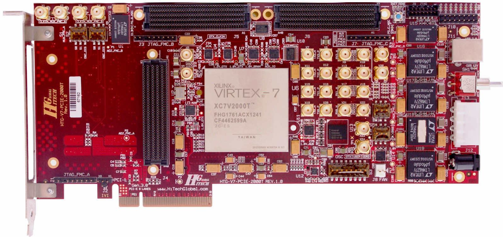
    HTG-700: Xilinx Virtex™ -7 PCI Express  Development Platform


    Powered by Xilinx Virtex-7 V2000T, V585, or X690T  the HTG-700 is ideal for ASIC/SOC prototyping, high-performance computing, high-end image processing, PCI Express Gen 2 & 3 development, general purpose FPGA development, and/or applications requiring high speed serial transceivers (up to 12.5Gbps).  

    Three High Pin Count (HPC) FMC connectors provide access to 480 single-ended I/Os and 24 high-speed Serial Transceivers of the on board Virtex 7 FPGA. Availability of over 100 different off-the-shelf FMC modules extend functionality of the board for variety of different applications. 


    Eight lane of PCI Express Gen 2 is supported by hard coded controllers inside the Virtex 7 FPGA. The board's layout, performance of the Virtex 7 FPGA fabric, high speed serial transceivers (used for PHY interface), flexible on-board clock/jitter attenuator, along with soft PCI Express Gen 3 IP core allow usage of the board for PCI Express Gen3 applications. 

    The HTG-700 Virtex 7 FPGA board can be used either in PCI Express mode (plugged into host PC/Server) or stand alone mode (powered by external ATX or wall power supply).


    Features:
    Xilinx Virtex-7 V2000T, 585T, or X690T FPGA
    Scalable via HTG-777 FPGA module  for providing higher FPGA gate density
    x8 PCI Express Gen2 /Gen 3  edge connectors with jitter cleaner chip
      - Gen 3: with the -690 option
      - Gen 2: with the -585 or -2000 option (Gen3 requires soft IP core)
    x3 FPGA Mezzanine Connectors (FMC)
      - FMC #1: 80 LVDS (160 single-ended) I/Os and 8 GTX (12.5 Gbps) Serial
        Transceivers
      - FMC #2: 80 LVDS (160 single-ended) I/Os and 8 GTX (12.5 Gbps) Serial
        Transceivers
      - FMC #3: 80 LVDS (160 single-ended) I/Os and 8 GTX (12.5 Gbps) Serial
        Transceivers. Physical location of this  connector allows  plug-in FMC
        daughter cards having easy access to the board through the front panel.
    x4 SMA ports (16 SMAs providing 4 Txn/Txp/Rxn/Rxp) clocked by external pulse generators
    DDR3 SODIMM with support for up to 8GB (shipped with a 2GB module)
    Programmable oscillators (Silicon Labs Si570) for different interfaces
    Configuration through JTAG or Micron G18 Embedded Flash
    USB to UART bridge
    ATX and DC power supplies for PCI Express and Stand Alone operations
    LEDs & Pushbuttons
    Size: 9.5" x 4.25"
    Kit Content:

    Hardware:
    -
    HTG-700 board

    Software:

    - PCI Express Drivers (evaluation) for Windows & Linux

    Reference Designs/Demos:
    - PCI Express Gen3 PIO
    - 10G & 40G Ethernet (available only if interested in licensing the IP cores)
    - DDR3 Memory Controller

    Documents:

    - User Manual
    - Schematics (in searchable .pdf format)
    - User Constraint File (UCF)

    Ordering information Part Numbers:
    - HTG-V7-PCIE-2000-2 (populated with V2000T-2 FPGA)
    Price:
    Contact Us
    -
    HTG-V7-PCIE-690-2   (populated with X690T-2 FPGA)  
    Price:
    Contact us
    - HTG-V7-PCIE-690-3   (populated with X690T-3 FPGA)  
    Price:
    Contact us
    -
    HTG-V7-PCIE-585-2   (populated with V585T-2 FPGA)
    Price:
    Contact us


    FPGA-(CVP-13, XUPVV4): Hardware Modifications


    Currently, (08d-10m-2018y), the Bittware cards (CVP-13, XUPVV4) do not require any modifications and will run at full speed out-of-the-box.

    If you have a VCU1525 or BCU1525, you should acquire a DC1613A USB dongle to change the core voltage.

    This dongle requires modifications to ‘fit’ into the connector on the VCU1525 or BCU1525.

    You can make the modifications yourself as described here,

    You can purchase buy a fully modified DC1613A from https://shop.fpga.guide.

    If you have an Avnet AES-KU040 and you are brave enough to make the complex modifications to run at full hash rate, you can download the modification guide right here (it will be online in a few days).

    You can see a video of the modded card On YouTube: Here.

    If you have a VCU1525 or BCU1525, we recommend using the TUL Water Block (this water block was designed by TUL, the company that designed the VCU/BCU cards).

    The water block can be purchased from https://shop.fpga.guide.


    WARNING:  Installation of the water block requires a full disassembly of the FPGA card which may void your warranty.

    Maximum hash rate (even beyond water-cooling) is achieved by immersion cooling, immersing the card in a non-conductive fluid.

    Engineering Fluids makes BC-888 and EC-100 fluids which are non-boiling and easy to use at home. You can buy them here.

    If you have a stock VCU1525, there is a danger of the power regulators failing from overheating, even if the FPGA is very cool.

     We recommend a simple modification to cool the power regulators by more than 10C.


    The modification is very simple. You need:
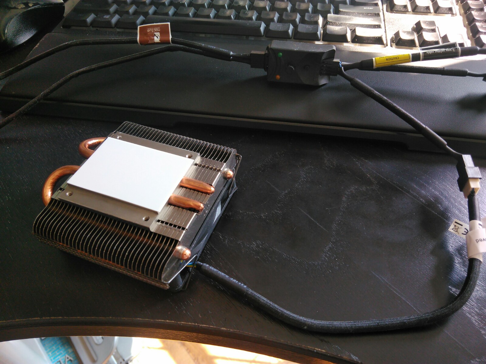
    First, cut a piece of thermal tape and apply it to the back side of the Slim X3 CPU cooler, and plug the fan into the fan controller:


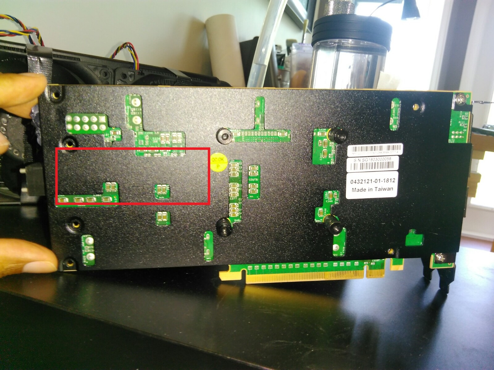
    Then, you are going to stick the CPU cooler on the back plate of the VCU1525 on this area:


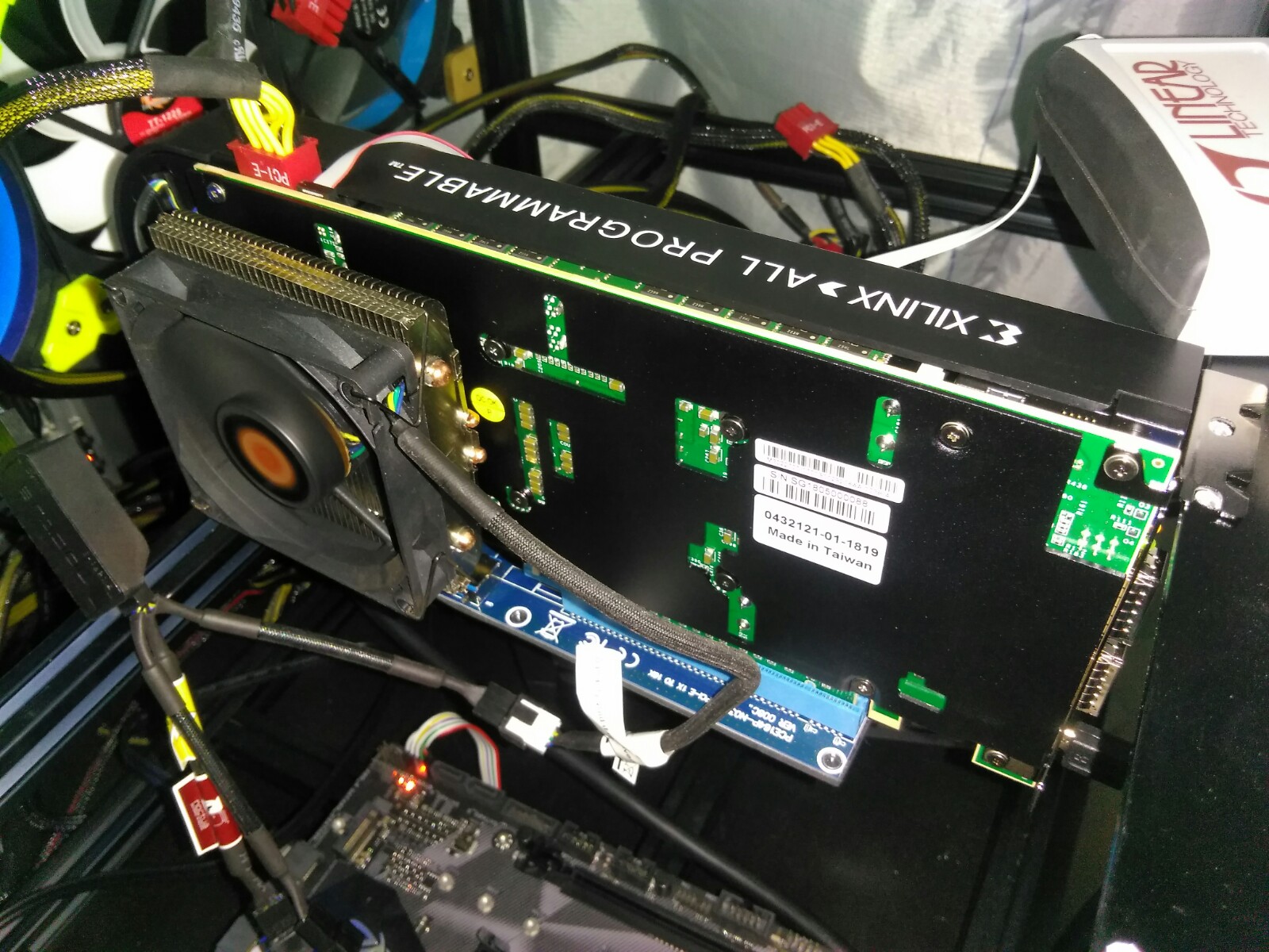
    Once done it will look like this:


    Make sure to connect the fan controller to the power supply and run the fan on maximum speed.

    This modification will cool the regulators on the back side of the VCU1525, dropping their temperature by more than 10C and extending the life of your hardware.

    This modification is not needed on ‘newer’ versions of the hardware such as the XBB1525 or BCU1525.


    OptEdited:

    Source-Page:
    Grab Bag of FPGA and GPU Software Tools from Intel, Xilinx & NVIDIA


    FPGA's as Accelerators:
    • From the Intel® FPGA SDK for OpenCL™ Product Brief available at link.
    • "The FPGA is designed to create custom hardware with each instruction being accelerated providing more efficiency use of the hardware than that of the CPU or GPU architecture would allow." 


    Hardware:
    • With Intel, developers can utilize an x86 with a built-in FPGA or connect a card with an Intel or Xilinx FPGA to an x86. This Host + FPGA Acceleration would typically be used in a "server."
    • With Intel and Xilinx, developers can also get a chip with an ARM core + FPGA. This FPGA + ARM SoC Acceleration is typically used in embedded systems.
    • Developers can also connect a GPU card from Nvidia to an x86 host. Developers can also get an integrated GPU from Intel. Nvidia also provides chips with ARM cores + GPUs.

    Tools:
    • Intel and Xilinx provide tools to help developers accelerate x86 code execution using an FPGA attached to the x86. They also provide tools to accelerate ARM code execution using an FPGA attached to the ARM.
    • Intel, Xilinx and Nvidia all provide OpenCL libraries to access their hardware. These libraries can not interoperate with one another. Intel also provides libraries to support OpenMP and Nvidia provides CUDA for programming their GPUS. Xilinx includes their OpenCL library in an SDK called SDAccel and an SDK called SDSoC. SDAccel is used for x86 + Xilinx FPGA systems, i.e. servers. SDSoC is used for Xilinx chips with ARM + FPGAs, i.e. embedded systems.

    Libraries:
    • To help developers building computer vision applications, Xilinx provides OpenVX, Caffe, OpenCV and various DNN and CNN libraries in an SDK called reVISION for software running on chips with an ARM+FPGA.
    • All of these libraries and many more are available for x86 systems.
    • Xilinx also provides neural network inference, HEVC decoders and encoders and SQL data-mover, function accelerator libraries.

    Tools for FPGA + ARM SoC Acceleration Intel:
    • From link developers can work with ARM SoCs from Intel using:
    • ARM DS-5 for debug
    • SoC FPGA Embedded Development Suite for embedded software development tools
    • Intel® Quartus® Prime Software for working with the programmable logic
    • Virtual Platform for simulating the ARM
    • SoC Linux for running Linux on the FPGA + ARM SoC
    • Higher Level
    • Intel® FPGA SDK for OpenCL™ is available for programming the ARM + FPGA chips using OpenCL.

    Xilinx:
    • Developers can work with ARM SoCs from Xilinx using:
    • An SDK for application development and debug
    • PetaLinux Tools for Linux development and ARM simulation and
    • Vivado for using the PL for working with its FPGA + ARM SoC chips


    Higher Level:
    • Xilinx provides SDSoC for accelerating ARM applications on the built-in FPGA. Users can program in C and/or C++ and SDSoC will automatically partition the algorithm between the ARM core and the FPGA. Developers can also program using OpenCL and SDSoC will link in an embedded OpenCL library and build the resulting ARM+FPGA system. SDSoC also supports debugging and profiling.


    Domain Specific:
    Xilinx leverages SDSoC to create an embedded vision stack called reVISION.


    Source-Website:

    SPINPACK

    spin system logo

    Author:
    Joerg Schulenburg, Uni-Magdeburg, 2008-2016


    What is SpinPack?

    SPINPACK is a big program package to compute lowest eigenvalues and eigenstates and various expectation values (spin correlations etc) for quantum spin systems.


    These model systems can for example describe magnetic properties of insulators at very low temperatures (T=0) where the magnetic moments of the particles form entangled quantum states.


    The package generates the symmetrized configuration vector, the sparse matrix representing the quantum interactions and computes its eigenvectors and finaly some expectation values for the system.

    The first SPINPACK version was based on Nishimori's TITPACK (Lanczos method, no symmetries), but it was early converted to C/C++ and completely rewritten (1994/1995).

    Other diagonalization algorithms are implemented too (Lanzcos, 2x2-diagonalization and LAPACK/BLAS for smaller systems). It is able to handle Heisenberg, t-J, and Hubbard-systems up to 64 sites or more using special compiler and CPU features (usually up to 128) or more sites in slower emulation mode (C++ required).

    For instance we got the lowest eigenstates for the Heisenberg Hamiltonian on a 40 site square lattice on our machines at 2002. Note that the resources needed for computation grow exponentially with the system size.

    The package is written mainly in C to get it running on all unix systems. C++ is only needed for complex eigenvectors and twisted boundary conditions when C has no complex extension. This way the package is very portable.

    Parallelization can be done using MPI- and PTHREAD-library. Mixed mode (hybrid mode) is possible, but not always faster than pure MPI (2015). v2.60 has slightly hybrid mode advantage on CPUs supporting hyper-threading.

    This will hopefully be improved further. MPI-scaling is tested to work up to 6000 cores, PTHREAD-scaling up to 510 cores but requires careful tuning (scaling 2008-1016).

    The program can use all topological symmetries, S(z) symmetry and spin inversion to reduce matrix size. This will reduce the needed computing recources by a linear factor.

    Since 2015/2016 CPU vector extensions (SIMD, SSE2, AVX2) are supported to get better performance doing symmetry operations on bit representations of the quantum spins.

    The results are very reliable because the package has been used since 1995 in scientific work. Low-latency High-bandwith network and low latency memory is needed to get best performance on large scale clusters.

    News:

    • Groundstate of the S=1/2 Heisenberg AFM on a N=42 kagome biggest sub-matrix computed (Sz=1 k=Pi/7 size=36.7e9, nnz=41.59, v2.56 cplx8, using partly non-blocking hybrid code on supermuc.phase1 10400cores(650 nodes, 2 tasks/node, 8cores/task, 2hyperthreads/core, 4h), matrix_storage=0.964e6nz/s/core SpMV=6.58e6nz/s/core Feb2017)
    • Groundstate of the S=1/2 Heisenberg AFM on a N=42 linear chain computed (E0/Nw=-0.22180752, Hsize = 3.2e9, v2.38, Jan2009) using 900 Nodes of a SiCortex SC5832 700MHz 4GB RAM/Node (320min).
      Update: N=41 Hsize = 6.6e9, E0/Nw=-0.22107343 16*(16cores+256GB+IB)*32h matrix stored, v2.41 Oct2011).
    • Groundstate of the S=1/2 Heisenberg AFM on a N=42 square lattice computed (E0 = -28.43433834, Hsize = 1602437797, ((7,3),(0,6)), v2.34, Apr2008) using 23 Nodes a 2*DualOpteron-2.2GHz 4GB RAM via 1Gb-eth (92Cores usage=80%, ca.60GB RAM, 80MB/s BW, 250h/100It).
    • Program is ready for cluster (MPI and Pthread can be used at the same time, see the performance graphic) and can again use memory as storage media for performance measurement (Dec07).
    • Groundstate of the S=1/2 Heisenberg AFM on a N=40 square lattice computed (E0 = -27.09485025, Hsize = 430909650, v1.9.3, Jan2002).
    • Groundstate of the S=1/2 J1-J2-Heisenberg AFM on a N=40 square lattice J2=0.5, zero-momentum space: E0= -19.96304839, Hsize = 430909650 (15GB memory, 185GB disk, v2.23, 60 iterations, 210h, Altix-330 IA64-1.5GHz, 2 CPUs, GCC-3.3, Jan06)
    • Groundstate of the S=1/2 Heisenberg AFM on a N=39 triangular lattice computed (E0 = -21.7060606, Hsize = 589088346, v2.19, Jan2004).
    • Largest complex Matrix: Hsize=1.2e9 (26GB memory, 288GB disk, v2.19 Jul2003), 90 iterations: 374h alpha-1GHz (with limited disk data rate, 4 CPUs, til4_36)
    • Largest real Matrix: Hsize=1.3e9 (18GB memory, 259GB disk, v2.21 Apr2004), 90 iterations: real=40h cpu=127h sys=9% alpha-1.15GHz (8 CPUs, til9_42z7) 

      Download:

      Verify download using: gpg --verify spinpack-2.55.tgz.asc spinpack-2.54.tgz


       Installation:

      • gunzip -c spinpack-xxx.tgz | tar -xf - # xxx is the version number
      • cd spinpack; ./configure --mpt
      • make test # to test the package and create exe path
      • # edit src/config.h exe/daten.def for your needs (see models/*.c)
      • make
      • cd exe; ./spin


      Documentation:

      The documentation is available in the doc-path. Most parts of the documentation are rewritten in english now.

      If you still find some parts written in german or out-of-date documentation send me an email with a short hint where I find this part and I want to rewrite this part as soon as I can.

      Please see doc/history.html for latest changes. You can find a documentation about speed in the package or an older version on this spinpack-speed-page.


      Most Important Function:

      The most time consuming important function is b_smallest in hilbert.c. This function computes the representator of a set of symmetric spin configurations (bit pattern) from a member of this set.

      It also returns a phase factor and the orbit length. It would be a great progress, if the performance of that function could be improved. Ideas are welcome.

      One of my motivations is to use FPGAs in 2009 was inspired by the FPGA/VHDL-Compiler.

      These are Xilings-tools and are so slow, badly scaling and buggy, that code generation and debugging is really no fun and a much better FPGA toolchain is needed for HPC, but all that is fixed now with updates.

      2015-05 I added software benes-network to get gain of AVX2, but it looks like that its still not the maximum available speed (HT shows near 2 factor, bitmask falls out of L1-cache?).

      Examples for open access

      Please use these data for your work or verify my data. Questions and corrections are welcome. If you miss data or explanations here, please send a note to me.


      Frequently asked questions (FAQ):

       Q: I try to diagonalize a 4-spin system, but I do not get the full spectrum. Why?
       A: Spinpack is designed to handle big systems. Therefore it uses as much
          symmetries as it can. The very small 4-spin system has a very special
          symmetry which makes it equivalent to a 2-spin system build by two s=1 spins.
          Spinpack uses this symmetry automatically to give you the possibility
          to emulate s=1 (or s=3/2,etc) spin systems by pairs of s=1/2 spins.
          If you want to switch this off, edit src/config.h and change
          CONFIG_S1SYM to CONFIG_NOS1SYM.


      This picture is showing a small sample of a possible Hilbert matrix. The non-zero elements are shown as black pixels (v2.33 Feb2008 kago36z14j2).

      Hilbert matrix N=36 s=1/2 kago lattice


      This picture is showing a small sample of a possible Hilbert matrix. The non-zero elements are shown as black (J1) and gray (J2) pixels (v2.42 Nov2011 j1j2-chain N=18 Sz=0 k=0). Config space is sorted by J1-Ising-model-Energy to show structures of the matrix. Ising energy ranges are shown as slightly grayed arrays.

      Hilbert matrix for N=18 s=1/2 quantum chain


      Ground state energy scaling for finite size spin=1/2-AFM-chains N=4..40 using up to 300GB memory to store the N=39 sparse matrix and 245 CPU-houres (2011, src=lc.gpl).
      ground state s=1/2-AFM-LC


      Author: Joerg Schulenburg, Uni-Magdeburg, 2008-2016


      XC7V2000T-x690T_HTG-700: Models

      FPGA Scematic Updates: Cryptocurrency

      Reference Materials

      FPGA Scematic Updates


      FPGA Device Driver Memo

      Contents

      [hide]

      FPGA device driver (Memory Mapped Kernel)


      Description

      A simple linux device driver for FPGA access. This driver provides memory mapped support and can communicate with FPGA designs. The advantage that memory mapping provides is that the system call overhead is completely reduced. However network overhead and the EPB bus bandwidth limitation exists. PowerPC in ROACH is mainly intended for control and monitoring. For larger transactions and performance numbers, the recommendation is to read the data directly from the FPGA through the 10Ge interface.

      Need for an alternate device driver

      BORPH software approach incurs system call latencies, which can degrade performance in applications that make frequent short or random accesses to FPGA resources. System calls are function invocations made from user-space in order to request some service from the operating system. Instead of making a series of system calls that involve file I/O, we memory map the FPGA to the user process address space in the PowerPC. Memory mapping forms an association between the FPGA and the user process memory. In doing so, the abstraction is being moved from the kernel to the user application. The performance of a memory mapped FPGA device is measurably better than the current approach of BORPH which presents a file system of hardware mapped registers. The contribution of a memory-mapped approach is two-fold: Firstly, the overhead of a system call performing I/O operations is eliminated. Secondly, unnecessary memory copies are not kept in the kernel. While the approach gives a performance benefit, it comes with the limitation that user applications are required to track and provide FPGA symbolic register name to memory to offset mapping. This limitation can be overcome by automating the mapping at FPGA design compile time in the same way as is currently done for BORPH, thereby abstracting this limitation away from ordinary users

      Advantages

      • Latest kernel support(Linux 3.10)
      • mmap method support
      • Improved performance
      • support for both ROACH and ROACH2 platforms

      Implications

      • Experimental
      (Let me know feedback at shanly@ska.ac.za to iron out bugs)

      Usage

      The linux kernel communicates with the FPGA through special files called "device nodes". There are two device nodes to be created.
      • /dev/roach/config (FPGA configuration)
      • /dev/roach/mem (FPGA read write)
      tcpborphserver3 communicates with FPGA through these device specific nodes.
      • telnet ip-address portno
      You will see the katcp commands by issuing ?help

      Kernel Source

      There is a working config file incase you struggle to build the kernel image from the source on your own. NOTE: Depending on platform use roach or roach2.
        • make 44x/roach_defconfig (for roach2, make 44x/roach2_defconfig)
        • make cuImage.roach (for roach2, make cuImage.roach2)
      (The kernel binary built can be located in arch/powerpc/boot/cuImage.roach) The driver can be found in drivers/char/roach directory.

      Steps to follow

      1. Build the kernel binary from source as indicated above OR use the provided kernel precompiled binary(uImage-roach-mmap) available after checking out the git repository below
        1. git clone https://github.com/shanlyrajan/roach2_linux
        2. Note the two files uImage-roach-mmap and test_mmap_RW after checking out.
      2. Run the below macro in uboot assuming you are nfs booting and you have placed the uImage-roach-mmap file in location from where tftp can fetch it.
        1. setenv roachboot "dhcp;tftpboot 0x2000000 uImage-roach-mmap; setenv bootargs console=ttyS0,115200 root=/dev/nfs ip=dhcp;bootm 0x2000000"
        2. saveenv to save the created macro to flash
        3. run roachboot
      3. Ignore the fatal module dep warning that you see after booting the kernel. After kernel boots in init prompt type the following. Once netbooted, mount the nfs filesystem rw. Create device files if not created, /dev/roach/config that is the programming bitstream interface and /dev/roach/mem that is the memory mapped read/write interface using mknod.
        1. cat /proc/devices (To see whether driver is loaded and check the major number associated with it. I would expect you to see 252 major number)
        2. mount -o rw,remount /
        3. mkdir /dev/roach
        4. mknod /dev/roach/config c 252 0
        5. mknod /dev/roach/mem c 252 1
        6. mount -o ro,remount /
      4. Use tcpborphserver3 available along with KATCP which has registername to offset support logic.
        1. Issue katcp commands like ?progdev x.bof, ?listdev, ?wordread and ?wordwrite for communicating with designs.

      Reference userspace code

      The test_mmap_RW.c available in the checked out source code, performs reading, writing and verifying the scratchpad register half a million times. The code can be used as a reference and adapted to read data out of BRAMs and send as UDP packets. Note: The c file has to be cross-compiled to run on powerpc platform and then the executable can run on the PowerPC itself. Core_info.tab is the authoritative source for checking the register name and memory offset into FPGA.
       

      FPGA Heterogeneous Self-Healing


      FPGA Autonomous Acceleration Self-Healing


      This example uses FPGA-in-the-Loop (FIL) simulation to accelerate a video processing simulation with Simulink® by adding an FPGA. The process shown analyzes a simple system that sharpens an RGB video input at 24 frames per second.
      This example uses the Computer Vision System Toolbox™ in conjunction with Simulink® HDL Coder™ and HDL Verifier™ to show a design workflow for implementing FIL simulation.


      Products required to run this example:
      • MATLAB
      • Simulink
      • Fixed-Point Designer
      • DSP System Toolbox
      • Computer Vision System Toolbox
      • HDL Verifier
      • HDL Coder
      • FPGA design software (Xilinx® ISE® or Vivado® design suite or Intel® Quartus® Prime design software)
      • One of the supported FPGA development boards and accessories (the ML403, SP601, BeMicro SDK, and Cyclone III Starter Kit boards are not supported for this example)
      • For connection using Ethernet: Gigabit Ethernet Adapter installed on host computer, Gigabit Ethernet crossover cable
      • For connection using JTAG: USB Blaster I or II cable and driver for Altera FPGA boards. Digilent® JTAG cable and driver for Xilinx FPGA boards.
      • For connection using PCI Express®: FPGA board installed into PCI Express slot of host computer.
      MATLAB® and FPGA design software can either be locally installed on your computer or on a network accessible device. If you use software from the network you will need a second network adapter installed in your computer to provide a private network to the FPGA development board. Consult the hardware and networking guides for your computer to learn how to install the network adapter.
      Note: The demonstration includes code generation. Simulink does not permit you to modify the MATLAB installation area. If necessary, change to a working directory that is not in the MATLAB installation area prior to starting this example.

      1. Open and Execute the Simulink Model

      Open the fil_videosharp_sim.mdl and run the simulation for 0.21s.

      Due to the large quantity of data to process , the simulation is not fluent. We will improve the simulation speed in the following steps by using a FPGA-in-the-Loop.

      2. Generate HDL Code

      Generate HDL code for the Streaming Video Sharpening subsystem by performing these steps:
      a. Right-click on the block labeled Streaming 2-D FIR Filter.
      b. Select HDL Code Generation > Generate HDL for Subsystem in the context menu.
      Alternatively, you can generate HDL code by entering the following command at the MATLAB prompt:
      >> makehdl('fil_videosharp_sim/Streaming 2-D FIR Filter')
      If you do not want to generate HDL code, you can copy pre-generated HDL files to the current directory using this command:
      >> copyFILDemoFiles('videosharp');

      3. Set Up FPGA Design Software

      Before using FPGA-in-the-Loop, make sure your system environment is set up properly for accessing FPGA design software. You can use the function hdlsetuptoolpath to add ISE or Quartus II to the system path for the current MATLAB session.
      For Xilinx FPGA boards, run
      hdlsetuptoolpath('ToolName', 'Xilinx ISE', 'ToolPath', 'C:\Xilinx\13.1\ISE_DS\ISE\bin\nt64\ise.exe');
      This example assumes that the Xilinx ISE executable is C:\Xilinx\13.1\ISE_DS\ISE\bin\nt64\ise.exe. Substitute with your actual executable if it is different.
      For Altera boards, run
      hdlsetuptoolpath('ToolName','Altera Quartus II','ToolPath','C:\altera\11.0\quartus\bin\quartus.exe');
      This example assumes that the Altera Quartus II executable is C:\altera\11.0\quartus\bin\quartus.exe. Substitute with your actual executable if it is different.

      4. Run FPGA-in-the-Loop Wizard

      To launch the FIL Wizard, select Tools > Verification Wizards > FPGA-in-the-Loop (FIL)... in the model window or enter the following command at the MATLAB prompt:
      >> filWizard;

      4.1 Hardware Options

      Select a board in the board list.

      4.2 Source Files

      a. Add the previously generated HDL source files for the Streaming Video Sharpening subsystem.
      b. Select Streaming_2_D_FIR_Filter.vhd as the Top-level file.

      4.3 DUT I/O Ports

      Do not change anything in this view.

      4.4 Build Options

      a. Select an output folder.
      b. Click Build to build the FIL block and the FPGA programming file.
      During the build process, the following actions occur:
      • A FIL block named Streaming_2_D_FIR_Filter is generated in a new model. Do not close this model.
      • After new model generation, the FIL Wizard opens a command window where the FPGA design software performs synthesis, fit, place-and-route, timing analysis, and FPGA programming file generation. When the FPGA design software process is finished, a message in the command window lets you know you can close the window. Close the window.
      c. Close the fil_videosharp_sim model.

      5. Open and Complete the Simulink Model for FIL

      a. Open the fil_videosharp_fpga.slx.
      b. Copy in it the previously generated FIL block to fil_videosharp_fpga.slx where it say "Replace this with FIL block"

      6. Configure FIL Block

      a. Double-click the FIL block in the Streaming Video Sharpening with FPGA-in-the-Loop model to open the block mask.
      b. Click Load.
      c. Click OK to close the block mask.

      7. Run FIL Simulation

      Run the simulation for 10s and observe the performance improvement.

      This concludes the Video Processing Acceleration using FPGA-In-the-Loop example.

      FPGA Monero Working IP-Cores Shares


      FPGA Monero Working IP-Cores Shares


      Build Status

      DownLoad - Click Here - SiaFpgaMiner

      This project is a VHDL FPGA core that implements an optimized Blake2b pipeline to mine Siacoin.

      Motivation

      When CPU mining got crowded in the earlier years of cryptocurrencies, many started mining Bitcoin with FPGAs. The time arrived when it made sense to invest millions in ASIC development, which outperformed FPGAs by several orders of magnitude, kicking them out of the game. The complexity and cost of developing ASICs monopolized Bitcoin mining, leading to relatively dangerous mining centralization. Therefore, emerging altcoins decided to base their PoW puzzle on other algorithms that wouldn't give ASICs an unfair advantage (i.e. ASIC-resistant). The most popular mechanism has been designing the algorithm to be memory-hard (i.e. dependent on memory accesses), which makes memory bandwith the computing bottleneck. This gives GPUs an edge over ASICS, effectively democratizing access to mining hardware since GPUs are consumer electronics. Ethereum is a clear example of it with its Ethash PoW algorithm.
      Siacoin is an example of a coin without a memory-hard PoW algorith and no ASIC miners some ASIC miners are being rolled out (see Obelisk and Antminer A3). So was a perfect candidate for FPGA mining! (more for fun than profit)

      Design theory

      To yield the highest posible hash rate, a fully unrolled pipeline was implemented with resources dedicated to every operation of every round of the Blake2b hash computation. It takes 96 clock cycles to fill the pipeline and start getting valid results (4 clocks per 'G' x 2 'G' per round x 12 rounds).
      • MixG.vhd implements the basic 'G' function in 4 steps. Eight and two-step variations were explored but four steps gave the best balance between resource usage and timing.
      • QuadG.vhd is just a wrapper that instantiates 4 MixG to process the full 16-word vectors and make the higher level files easier to understand.
      • Blake2bMinerCore.vhd instantiates the MixG components for all rounds and wires their inputs and outputs appropiately. Nonce generation and distribution logic also lives in this file.
      • /Example contains an example instantiation of Blake2bMinerCore interfacing a host via UART. It includes a very minimalist Python script to interface the FPGA to a Sia node for mining.

      MixG

      The diagram below shows the pipeline structure of a single MixG. Four of these are instantiated in parall to constitute QuadGs, which are chained in series to form rounds.
      MixG logic
      The gray A, B, C, D boxes contain combinatorial operations to add and rotate bits according to the G function specification. The white two-cell boxes represent two 64-bit pipelining registers to store results from the combinatorial logic that are used later on the process.

      Nonce Generation and Distribution

      Pipelining the hash vector throughout the chain implies heavy register usage and there is no way around it. Fortunately the X/Y message feeds aren't as resource-demanding because the work header can remain constant for a given block period, with the exception of the nonce field, which must obviously be changing all the time to yield unique hashes. Therefore, the nonce field must be tracked or kept in memory for when a given step in the mixing logic requires it. The most simplistic approach would be to make a huge N-bit wide shift register to "drag" the nonce corresponding to each clock cycle across the pipeline. This is not an ideal solution, for we would require N flip-flops (e.g. 48-bit counter) times the number of clock cycles it takes to cross the pipeline (48 x 96 = 4608 FF!)
      Luckily, the nonce field is only used once per round (12 times total). This allows hooking up 12 counters statically to the X or Y input where the nonce part of the message is fed in each round. To make the counter output the value of the nonce corresponding to a given cycle, the counters' initial values are offset by the amount of clock cycles between them. The following diagram illustrates the point:
      Nonce counters
      In this case the offsets show that the nonce used in round zero will be consumed by round one 8 clock cycles after, by round two 20 cycles after, and so on. (The distance in clock cycles between counters is defined by the Blake2b message schedule)

      Implementation results

      It is evident that a single core is too big to fit in a regular affordable FPGA device. A ballpark estimate of the flip-flop resources a single core could use:
      • 64-bits per word x 16 word registers per MixG x 4 MixG per QuadG x 2 QuadG per round x 12 rounds = 98,308 registers (not considering nonce counters and other pieces of logic).
      The design won't fit in your regular Spartan 6 dev board, which is why I built it for a Kintex 7 410 FPGA. Here are some of my compile tests:
      CoresClockHashrateMix stepsStrategyUtilizationWorst Setup SlackWorst Hold SlackFailuresNotes
      12002004Default18.00%0.1680
      22004004Default38.00%0
      32006004Default56.00%-0.246602 failing endpoints
      32006004Explore56.00%-0.2460.011602 failing endpoints
      3166.67500.014Default56.00%0.1320.020
      4166.67666.684Default75.00%0.0510.0090
      51668304ExplorePlacing error
      4173.33693.324Explore75.00%0.03900
      4173.33693.324Explore75.00%0.170.02201 BUFGs per core
      As seen in the table, the highest number of cores I was able to instantiate was 4 and the highest clock flequency that met timing was 173.33 MHz.
      ~700 MH/s is no better than a mediocre GPU, but power draw is way less! (hey, I did say it was for fun)

      Further work

      • Investigate BRAM as alternative to flip-flops (unlikely to fit the needs of this application).
      • Fine-tune a higher clock frequency to squeeze out a few more MH/s.
      • Porting to Blake-256 for Decred mining. That variant adds two rounds but words are half as wide, so fitting ~2x the number of cores sounds possible.
      • Do more in-depth tests with different number of steps in the G function (timing-resources tradeoff).
      • Play more with custom implementation strategies.

      Resources